
Manufacturing method of backside illuminated and electronic impact type CMOS sensors, pixel and sensor

A technology of CMOS sensor and manufacturing method, which is applied in the direction of electric solid-state devices, circuits, electrical components, etc., can solve the problems such as offset, increase of deviation, and no record of analog circuit characteristics that are not recorded.

Pending Publication Date: 2021-06-18
长春长光辰芯光电技术有限公司(日本)
View PDF6 Cites 0 Cited by
  • Summary
  • Abstract
  • Description
  • Claims
  • Application Information

AI Technical Summary

Problems solved by technology

In Patent Document 2 and Patent Document 3, the thickness of the silicon substrate is not described, but since there is no description of the shift in the characteristics of the analog circuit, the increase in variation, etc., the thickness of the silicon substrate is considered to be about the same as in Patent Document 1.
[0038] In addition, in the laser annealing system described in Patent Document 4, the device wafer 10m is also described as having a thickness TH in the range of about 10 μm to 100 μm, and there is no study on a silicon wafer smaller than 10 μm.
[0039] In addition, in Patent Documents 1 to 4, laser annealing is performed on all bonded wafers, but there is no description on the explosion of voids in bonded wafers by laser annealing, etc.
[0040] In addition, in the electron impact type CMOS sensors described in Patent Documents 5 and 6 and Non-Patent Document 1, it is also considered that a CMOS sensor using a silicon substrate of the plane is used. Problems in the case of electronics are not recorded

Method used


Image

  • Manufacturing method of backside illuminated and electronic impact type CMOS sensors, pixel and sensor
  • Manufacturing method of backside illuminated and electronic impact type CMOS sensors, pixel and sensor
  • Manufacturing method of backside illuminated and electronic impact type CMOS sensors, pixel and sensor

Examples


no. 1 approach

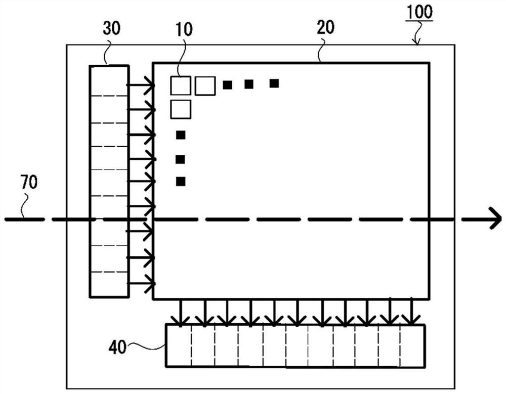
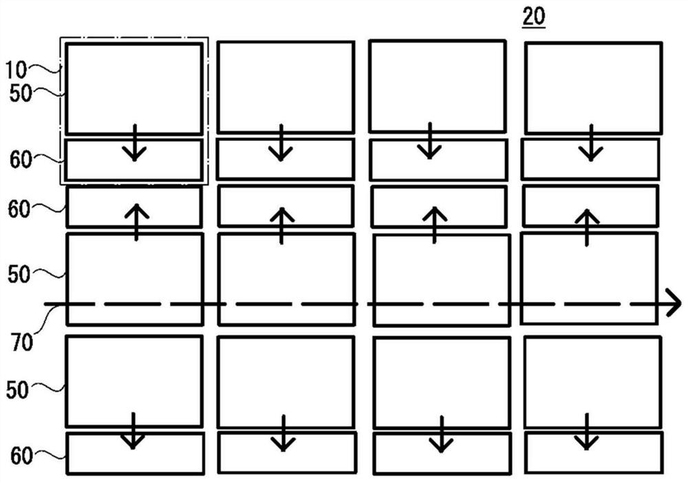
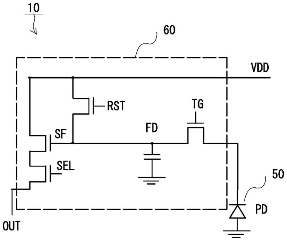
[0158] figure 1 is a schematic plan view of the back-illuminated CMOS sensor 100 of the first embodiment viewed from the front side, figure 2 is a schematic plan view showing an example of the arrangement of the photosensitive region 50 and the readout circuit 60 in the pixel region 20 of the back-illuminated CMOS sensor 100, image 3 is a schematic circuit diagram showing the structure of a pixel 10 of a back-illuminated CMOS sensor 100, Figure 4 is a schematic cross-sectional view around the photosensitive region 50 of the back-illuminated CMOS sensor 100 .

[0159] (Configuration of back-illuminated CMOS sensor 100 )

[0160] figure 1 An example of the overall configuration of the back-illuminated CMOS sensor 100 is shown. The back-illuminated CMOS sensor 100 is composed of a pixel area 20, a digital circuit 30 (vertical selection circuit, etc.) and an analog circuit 40 (sample-and-hold circuit, AD converter, etc.), and in the pixel area 20, the pixels 10 are horizont...

no. 2 approach

[0193] Figure 5 It is a schematic diagram showing the relationship between the position of the void 130 in the silicon wafer 110 and the laser irradiation region 120 in the second embodiment.

[0194] In general, the back-illuminated CMOS sensor 100 improves physical strength by bonding the surface side of the silicon wafer 110 on which the photosensitive region 50 or the readout circuit 60 and the like are formed to a silicon wafer serving as the supporting substrate 310 . However, when the silicon wafers are bonded together, voids 130 (voids) are generated at the bonding interface. In particular, at the wafer perimeter, particles attach, and small air bubbles are enclosed along the wafer perimeter, creating more voids 130 .

[0195] Furthermore, when the laser beam is irradiated to the part of the cavity 130 where the wafer is bonded, the gas etc. enclosed in the cavity 130 will expand rapidly, and the periphery of the cavity 130 will be in an explosive state, and silicon ...

no. 3 approach

[0201] Figure 6 It is a graph showing the difference in the distribution of ion-implanted boron depending on the presence or absence of an oxide film.

[0202] The manufacturing method of the back-illuminated CMOS sensor 100 according to the third embodiment relates to a method of implanting boron ions into the back surface of the back-illuminated CMOS sensor 100 .

[0203] Such as Figure 4 As shown, a P+ diffusion layer 270 is formed on the back surface (light-incident surface) of the photosensitive region 50 . This is to make the electrons of the electron-hole pairs generated at the interface on the back surface disappear by recombination with the holes in the P+ diffusion layer 270 so as not to become dark current.

[0204] On the other hand, when incident photons are photoelectrically converted inside the P+ diffusion layer 270 , the back-illuminated CMOS sensor 100 cannot detect the photons. In addition, when the back-illuminated CMOS sensor 100 is used as the sensor...


PUM

PropertyMeasurementUnit
thicknessaaaaaaaaaa

Abstract

The invention provides a manufacturing method of a backside illuminated CMOS sensor and a method for manufacturing an electron impact CMOS sensor, wherein the backside illuminated CMOS sensor and the electron impact CMOS sensor are capable of suppressing variation and increase of variation of characteristics of an analog circuit formed on a surface. This method for manufacturing a backside illuminated CMOS sensor (100) comprises: a formation step in which an N-type photosensitive region (50) is formed inside a silicon substrate (305); an implantation step in which ions for forming a P + diffusion layer (270) are implanted into the back surface of the silicon substrate (305); and an irradiation step in which laser light is irradiated from the back surface in order to activate the implanted ions, wherein the laser light is irradiated to the back-illuminated CMOS sensor (100) excluding the region where the analog circuit (40) is formed on the surface.

Description

technical field [0001] The invention relates to a method for manufacturing a back-illuminated CMOS sensor, a method for manufacturing an electron bombarded CMOS sensor, pixels for a back-illuminated CMOS sensor, and an electron bombarded CMOS sensor. Background technique [0002] The following patent documents are disclosed regarding the back-illuminated CMOS sensor and the manufacturing method of the back-illuminated CMOS sensor. [0003] For example, in Patent Document 1 (Japanese Patent Laid-Open No. 2003-031785 ), incident light is captured into the pixel structure of a photodiode through a wiring layer as a solution to the problem that part of the light condensed by the microlens is reflected by the wiring. As means, the following X-Y address type solid-state imaging device and its manufacturing method are disclosed. [0004] The solid-state imaging device described in Patent Document 1 is an X-Y address type solid-state imaging device in which unit pixels including ac...

Claims


Application Information

Patent Timeline
Patent Type & Authority Applications(China)
IPC IPC(8): H01L27/146
CPCH01L27/1464H01L27/14605H01L27/1463H01L27/14636H01L27/14687H01L27/14658
Inventor 木村雅俊周泉王欣洋
Owner 长春长光辰芯光电技术有限公司(日本)
Learn More