Infrared sensor

a technology of infrared sensors and sensors, applied in the field of infrared sensors, can solve the problems of difficult to achieve a thin profile (low profile), and achieve the effect of inhibiting the deterioration of sensitivity

Inactive Publication Date: 2015-07-07
PANASONIC INTELLECTUAL PROPERTY MANAGEMENT CO LTD
View PDF40 Cites 0 Cited by
  • Summary
  • Abstract
  • Description
  • Claims
  • Application Information

AI Technical Summary

Benefits of technology

[0010]In view of the above insufficiency, the present invention has been aimed to propose an infrared sensor which can be downsized and inhibit the deterioration of sensitivity caused by the capacitive coupling of the pyroelectric element and the output wiring connected to the IC device.Means for Solving the Problems

Problems solved by technology

Nevertheless, with the infrared sensor configured as shown in FIG. 12, it is difficult to achieve a thin profile (low profile) since the three-dimensional circuit block 120 is housed in the can package 130, and, furthermore, surface mounting is not possible when the infrared sensor is to be secondarily mounted on a circuit board such as a printed-wiring board.
Moreover, also with the infrared sensor configured as shown in FIG. 13, it is difficult to achieve a thin profile (low profile) since the simultaneously-formed molding 210 is housed in the can package 230, and, furthermore, surface mounting is not possible when the infrared sensor is to be secondarily mounted on a circuit board such as a printed-wiring board.
Meanwhile, with the infrared sensor configured as shown in FIG. 15 and FIG. 16, there is a limit to the improvement of the S / N ratio since the thermal noise that is generated by the resistor having a high resistance value will increase.
Nevertheless, in the foregoing case, since the infrared sensor element 301 and the IC device 102 or the IC device 202 need to be arranged in parallel next to each other in the package 303, it is difficult to achieve downsizing and cost reduction.

Method used


Image

  • Infrared sensor
  • Infrared sensor
  • Infrared sensor

Examples


embodiment 1

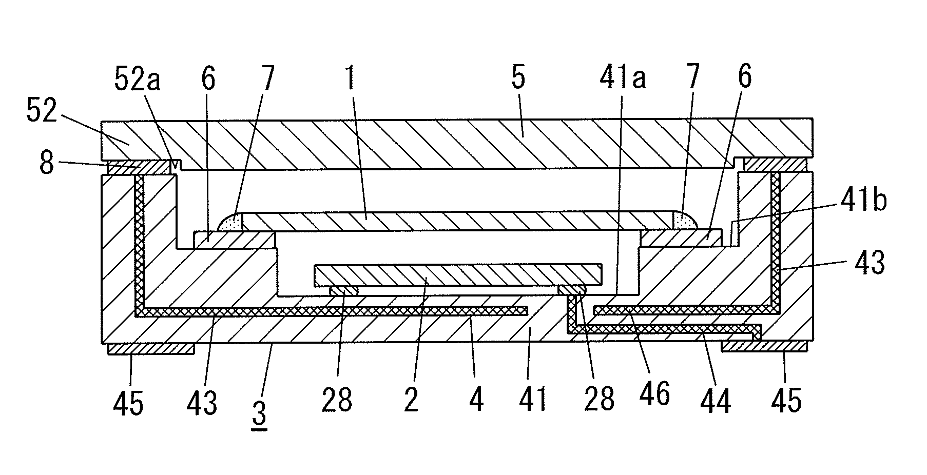
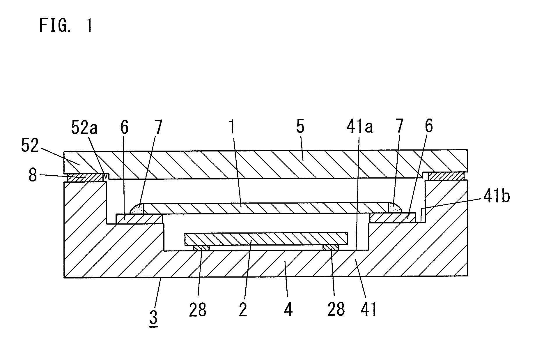
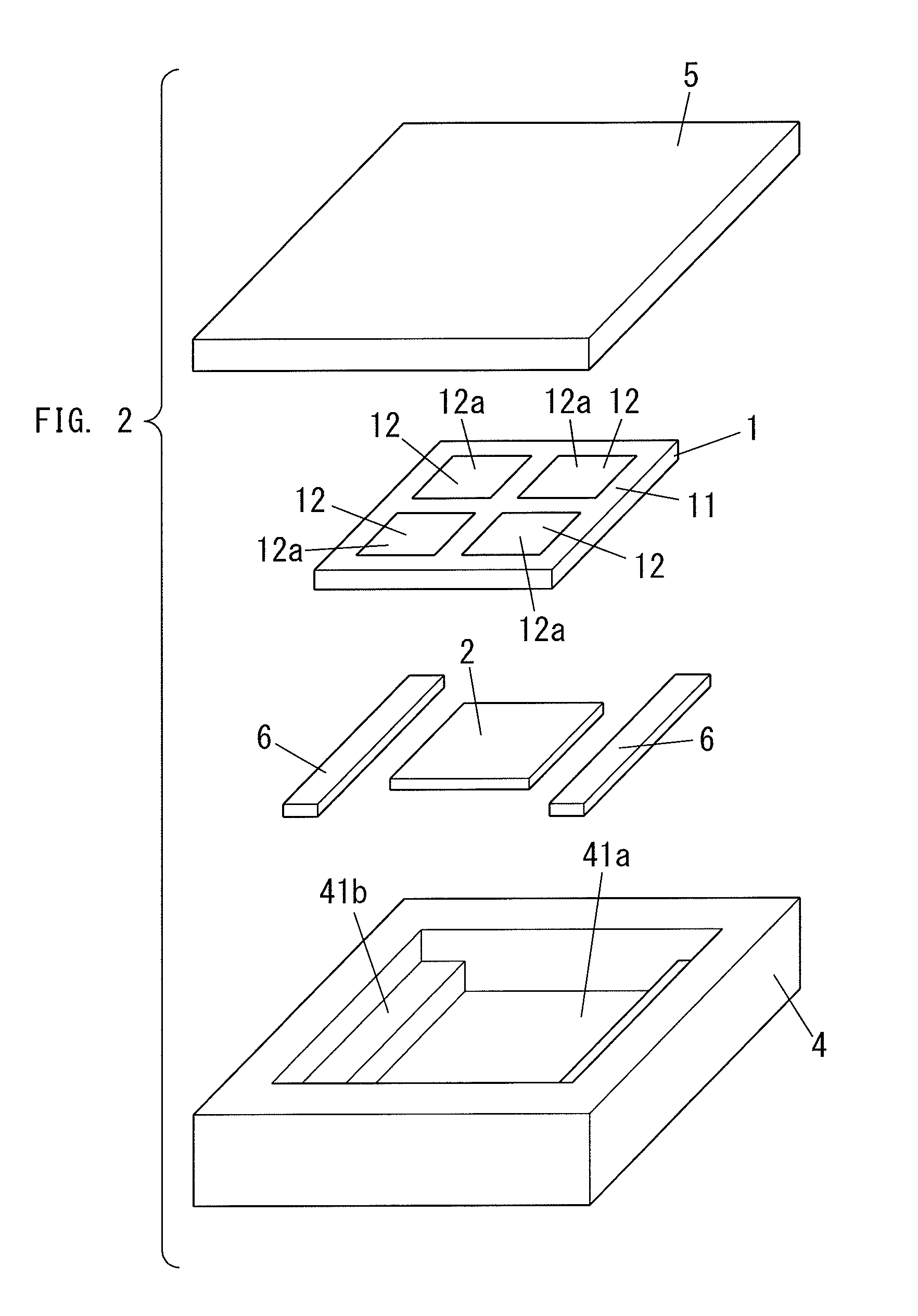
[0042]The infrared sensor of the present embodiment is now explained with reference to FIG. 1 to FIG. 4.

[0043]The infrared sensor of the present embodiment includes a pyroelectric element 1 as a thermal infrared detection element, an IC device 2 configured to process an output signal of the pyroelectric element 1, and a surface-mounted package 3 configured to house the pyroelectric element 1 and the IC device 2.

[0044]Here, the package 3 includes a package body 4, and a package lid 5. The package lid 5 is bonded to the package body 4 in a manner of enclosing the pyroelectric element 1 and the IC device 2 with the package body 4. The package body 4 includes a substrate 41, a circuit wiring (not shown), and a plurality of external connection electrodes 45 (refer to FIG. 4). The substrate 41 is made of a dielectric material (e.g., ceramics). The circuit wiring and the external connection electrodes 45 are made of a metal material and are formed on the substrate 41. The package lid 5 is ...

embodiment 2

[0081]The infrared sensor of the present embodiment has the substantially same basic configuration as Embodiment 1. As shown in FIG. 8, the infrared sensor of the present embodiment is different from Embodiment 1 in that the infrared sensor of the present embodiment includes, as the shielding member, a shield plate 30. The shield plate 30 is disposed between the rear surface of the IC device 2 and the pyroelectric element 1, thereby being positioned between the pyroelectric element 1 and the output wiring 44 (refer to FIG. 4). Note that the same components as Embodiment 1 are designated by the same reference numerals and explanations thereof are deemed unnecessary. Moreover, in FIG. 8, the illustration of the output wiring 44, the external connection electrodes 45, and the shield part 43 of FIG. 4 explained in Embodiment 1 is omitted.

[0082]In relation to the infrared sensor of the present embodiment, both ends of the shield plate 30 are fixed to respective parts near the lower reces...

embodiment 3

[0085]The basic configuration of the infrared sensor of the present embodiment shown in FIG. 9 is substantially the same as Embodiment 1, but differs in that the package lid 5 is a silicon lens. Note that the same reference numeral is given to the same constituent elements as Embodiment 1, and the explanation thereof is omitted. Moreover, in FIG. 9, the illustration of the output wiring 44, the electrodes for external connection 45, and the shield part 43 of FIG. 4 explained in Embodiment 1 is omitted. Moreover, the shielding member is provided in a similar manner as the other embodiments.

[0086]With the package lid 5 in the present embodiment, the center part defines a planar convex lens part 51, and the peripheral part 52 defines a flange part used for mounting the package lid 5 on the package body 4.

[0087]With regard to the infrared sensor of the present embodiment, the package lid 5 is a silicon lens. Therefore, high sensitivity can be achieved based on the improvement of the lig...


PUM


Abstract

The infrared sensor in accordance with the present invention includes a pyroelectric element, an IC device, and a surface-mounted package. The IC device is configured to process an output signal of the pyroelectric element. The package houses the pyroelectric element and the IC device. The package includes a package body and a package lid configured to transmit infrared rays to be detected by the pyroelectric element, and has electrical conductivity. The package body is provided on its surface with plural recessed parts arranged in tiers. The IC device is mounted on a bottom of the lower recessed part. The package body includes an output wiring configured to electrically connect an output terminal of the IC device to an external connection terminal and a shielding member interposed between the pyroelectric element and the output wiring.

Description

TECHNICAL FIELD[0001]The present invention relates to infrared sensors.BACKGROUND ART[0002]Conventionally, as shown in FIG. 12, proposed is an infrared sensor which houses, in a can package 130, a pyroelectric element 101, an IC device 102 in which most of the signal processing circuit that signal-processes an output current of the pyroelectric element 101 is integrated onto one chip, and a three-dimensional circuit block 120 made from an MID (Molded Interconnect Devices) substrate mounted with a capacitor (not shown) and the like attached outside the IC device 102 (for example, refer to Japanese Patent Publication No. 3367876; hereinafter referred to as “Patent Document 1”). Here, with the MID substrate configuring the three-dimensional circuit block 120, a circuit pattern 122 is formed on a surface of a resin molding 121. Moreover, the can package 130 is configured from a metal stem 131, and a metal cap 132 having an optical filter window 132a. Moreover, with the infrared sensor s...

Claims


Application Information

Patent Timeline
Patent Type & Authority Patents(United States)
IPC IPC(8): G01J5/10G01J5/06G01J5/04G01J5/34G01J5/08
CPCG01J5/34G01J5/04G01J5/045G01J5/048G01J5/06G01J5/08G01J5/0806G01J5/0875G01J5/0881G01J5/0893H01L2224/16225G01J1/02H10N15/10
Inventor NISHIKAWA, TAKAYUKITAWARATSUMIDA, SUKOYASUMI, SADAYUKI
Owner PANASONIC INTELLECTUAL PROPERTY MANAGEMENT CO LTD
Why Eureka
Try Eureka