Anti-fingerprint film, glass product and preparation method thereof
An anti-fingerprint film and glass product technology, which is applied in vacuum evaporation coating, coating, sputtering coating, etc., can solve the problem of weakened bonding strength between the film layer and the glass substrate, low friction resistance of the anti-fingerprint film, film Layer detachment from the base material and other problems, to achieve the effect of eliminating the problem of charge accumulation, long bonding strength, and simple process
- Summary
- Abstract
- Description
- Claims
- Application Information
AI Technical Summary
Problems solved by technology
Method used
Image

Examples
preparation example Construction
[0063] A method for preparing the glass product, comprising:
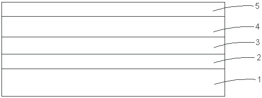
[0064] The conductive film layer, the transition layer, the silicon dioxide layer and the anti-fingerprint film layer are sequentially prepared on the glass substrate by magnetron sputtering.
[0065] In an optional embodiment, the initial vacuum of the magnetron sputtering is less than or equal to 5.0e -3 Pa;
[0066] In an optional embodiment, an ion source treatment is performed on the surface of the glass substrate before preparing the conductive film layer;
[0067] In an optional embodiment, the ion source operating voltage of the primary ion source treatment is 800-1200V, the current is 0.8-2.0A, and the treatment time is 5-15min;
[0068] Optionally, the ion source operating voltage for the primary ion source treatment can be any value between 800V, 900V, 1000V, 1100V, 1200V, and 800-1200V; the ion source operating current for the primary ion source treatment can be 0.8A , 1.0A, 1.5A, 2.0A and any value ...
Embodiment 1
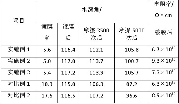
[0088] In this embodiment, the glass product of the front cover of the mobile phone made of AGC material is selected, and the initial water drop angle of the glass product before coating is measured after the two cleaning processes described in the present invention (see Table 1).
[0089] Place the cleaned glass products in a vacuum coating machine for coating. The specific process conditions are as follows:
[0090] 1. Vacuuming, the initial vacuum is 5.0e -3 Pa;
[0091] 2. Primary ion source treatment: using a linear ion source, under the condition of argon gas flow rate of 300 sccm and oxygen flow rate of 70 sccm, the plasma bombardment glass surface is generated at a voltage of 1000 V to clean the glass surface, and the processing time is 600 s , the actual output current is about 1.0 A;
[0092] 3. Conductive film layer: tin-indium alloy metal target, target power 4500 W, argon gas flow rate 300 sccm, oxygen flow rate 20 sccm, coating time 120s;
[0093] 4. Transiti...
Embodiment 2
[0101] The sample of this example was prepared by the same method as in Example 1, wherein the coating time of the conductive film layer was 65 s, the coating time of silicon dioxide was 500 s, and the rest of the conditions were unchanged.
[0102] In this embodiment, the thickness of the single layer is measured by a scanning electron microscope, wherein the thickness of the conductive film layer is about 3nm, the thickness of the transition layer is about 3nm, and the thickness of the SiO 2 The thickness of the layer is about 8nm, and the thickness of the anti-fingerprint film is about 24.6 nm. See Table 1 for the water drop angle of glass products after coating.
PUM
| Property | Measurement | Unit |
|---|---|---|
| thickness | aaaaa | aaaaa |
| thickness | aaaaa | aaaaa |
| thickness | aaaaa | aaaaa |
Abstract
Description
Claims
Application Information
 - R&D
- Intellectual Property
- Life Sciences
- Materials
- Tech Scout
- Unparalleled Data Quality
- Higher Quality Content
- 60% Fewer Hallucinations
Browse by: Latest US Patents, China's latest patents, Technical Efficacy Thesaurus, Application Domain, Technology Topic, Popular Technical Reports.
© 2025 PatSnap. All rights reserved.Legal|Privacy policy|Modern Slavery Act Transparency Statement|Sitemap|About US| Contact US: help@patsnap.com