


Quick Research
Generate reliable direction feasibility study reports for your R&D in just a few steps.

Technical Q&A
Discover and master advanced knowledge NOW. Basics, ideas, possibilities, all at once.

Find Solutions
As an expert in R&D theories, this can generate solutions to your technical problems instantly.

Evaluate Feasibility
Analyze your overall solution with one click, know your potential R&D risks in advance.

Monitor Landscape
Get weekly tech updates, stay abreast of the latest tech innovations and key insights.
Diamond circuit board preparation method based on laser direct processing
A laser direct, diamond technology, applied in the direction of printed circuit manufacturing, printed circuit, electrical components, etc., can solve the problems of high equipment requirements, complex and cumbersome preparation process, environmental hazard waste liquid, etc., achieve excellent performance, simple process, super Effect of High Heat Dissipation Performance
- Summary
- Abstract
- Description
- Claims
- Application Information
AI Technical Summary
Problems solved by technology
Method used
Image

Examples
Embodiment 1
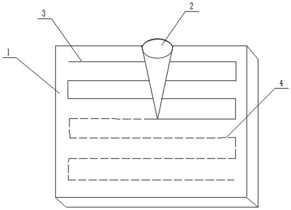
[0025] The diamond circuit board is prepared by the diamond circuit board preparation method based on laser direct processing, and the specific steps are as follows:
[0026] Select a diamond sheet with a size of 10mm×10mm×1mm, and perform pretreatment on the diamond sheet. Firstly, use 500 mesh and 1000 mesh SiC sandpaper to mechanically grind the diamond substrate, and then use 3 μm diamond grinding paste to polish, and finally Soak the polished diamond substrate in acetone, ethanol and deionized water respectively, and ultrasonically clean it for 10 minutes to produce a flat sheet substrate. The surface roughness Ra of the pretreated diamond substrate is 0.009±0.002 μm, and the thermal conductivity is 2000~2400W / (m K); put the pretreated substrate under the laser irradiation, the laser irradiation is carried out under the protection of high-purity argon, the laser power is 500W, the scanning speed is 500μm / s, and the spot diameter is 1000μm. A graphitized modified layer is ...
Embodiment 2
[0029] The difference from Example 1 is that the laser power of Example 2 is 200W, the spot diameter is 500 μm, and other conditions are the same as Example 1.
[0030] In Example 2, a diamond substrate with graphite wires on the surface was also obtained, but the width of the graphite wires was different, and the final measured width was 500 μm. Compared with Example 1, the width of the graphite wire is reduced, which improves its high-density interconnection; the prepared diamond circuit board has the characteristics of high heat dissipation performance and high-density interconnection structure.
Embodiment 3
[0032] The difference from Example 1 is that the laser power of Example 3 is 100W, the spot diameter is 200 μm, and other conditions are the same as those of Example 1.
[0033] In Example 3, a diamond substrate with graphite wires on the surface was also obtained, but the width of the graphite wires was different, and the final measured width was 200 μm. Compared with Example 1, the width of the graphite wire is reduced, which improves its high-density interconnection; the prepared diamond circuit board has the characteristics of high heat dissipation performance and high-density interconnection structure.
PUM
| Property | Measurement | Unit |
|---|---|---|
| surface roughness | aaaaa | aaaaa |
| diameter | aaaaa | aaaaa |
| diameter | aaaaa | aaaaa |
Abstract
Description
Claims
Application Information
 - R&D Engineer
- R&D Manager
- IP Professional
- Industry Leading Data Capabilities
- Powerful AI technology
- Patent DNA Extraction
Browse by: Latest US Patents, China's latest patents, Technical Efficacy Thesaurus, Application Domain, Technology Topic, Popular Technical Reports.
© 2024 PatSnap. All rights reserved.Legal|Privacy policy|Modern Slavery Act Transparency Statement|Sitemap|About US| Contact US: help@patsnap.com