
Gallium polar surface gallium nitride material and homoepitaxial growth method

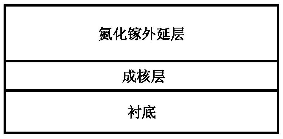
A technology of gallium nitride and gallium polarity, which is applied in electrical components, semiconductor/solid-state device manufacturing, circuits, etc., can solve problems such as changing growth temperature and switching air flow, reducing device breakdown voltage, and rough surface morphology of materials. Achieve the effects of reducing material dislocation density, increasing device breakdown voltage, and improving surface morphology

Pending Publication Date: 2021-05-04
XIDIAN UNIV
View PDF9 Cites 1 Cited by
  • Summary
  • Abstract
  • Description
  • Claims
  • Application Information

AI Technical Summary

Problems solved by technology

[0004] 1. Heteroepitaxial gallium polar surface gallium nitride materials need to adopt a nucleation layer structure, but the nucleation layer structure is easy to form a lateral leakage channel, which reduces the breakdown voltage of the device, and its growth conditions need to be precisely controlled, and the growth repeatability is poor. difficult to control;
[0005] 2. There are high-density dislocation defects in heteroepitaxial gallium polar surface gallium nitride materials, which will make the surface of the material rough, form pit-like defects and surface leakage channels, and reduce the breakdown voltage of the device;
[0006] 3. Dislocations in heteroepitaxial gallium polar surface gallium nitride materials are easy to capture electrons, resulting in device current collapse;
[0007] 4. In the heteroepitaxial gallium polar surface gallium nitride material, the growth parameters of the nucleation layer and the gallium polar surface gallium nitride material are different. It is necessary to change the growth temperature and switch the gas flow, and the growth process requires short pauses and intervals

Method used


Image

  • Gallium polar surface gallium nitride material and homoepitaxial growth method
  • Gallium polar surface gallium nitride material and homoepitaxial growth method
  • Gallium polar surface gallium nitride material and homoepitaxial growth method

Examples


Embodiment 1

[0031] Example 1, the fabrication substrate is gallium polar c-plane gallium nitride single crystal, and the transition layer is In 0.17 al 0.83 N, the epitaxial layer is gallium nitride material on the gallium polar surface of gallium nitride.

[0032] In step 1, a gallium polar c-plane gallium nitride single crystal is selected as the substrate, such as image 3 (a).

[0033] Step 2, epitaxy In 0.17 al 0.83 N transition layers, such as image 3 (b).

[0034] Place the substrate substrate in the reaction chamber, set the temperature at 660°C, the flow rate of nitrogen gas at 2.3 sccm, and the equilibrium vapor pressure of indium beam at 1.4×10 -7 Torr, the equilibrium vapor pressure of an aluminum beam is 1.5×10 -7 Torr, nitrogen RF source power of 375W process conditions, using molecular beam epitaxy technology, deposited In with a thickness of 10nm on a gallium polar c-plane gallium nitride single crystal substrate 0.17 al 0.83 N transition layer.

[0035] Step 3,...

Embodiment 2

[0037] Example 2, the fabrication substrate is gallium polar c-plane gallium nitride single crystal, and the transition layer is Sc with a thickness of 5nm 0.18 al 0.82 N, the epitaxial layer is gallium nitride material on the gallium polar surface of gallium nitride.

[0038] Step 1, choose gallium polar c-plane gallium nitride single crystal as the substrate, such as image 3 (a).

[0039] Step 2, epitaxial Sc 0.18 al 0.82 N transition layers, such as image 3 (b).

[0040] Place the substrate in the reaction chamber, set the temperature at 680°C, nitrogen flow at 2.3sccm, scandium beam equilibrium vapor pressure at 1.8×10 -8 Torr, the equilibrium vapor pressure of an aluminum beam is 1.4×10 -7 Torr, the nitrogen RF source power is 375W, and the molecular beam epitaxy technology is used to deposit Sc with a thickness of 5nm on the gallium polar c-plane gallium nitride single crystal substrate. 0.18 al 0.82 N transition layer.

[0041] Step 3, using molecular beam e...

Embodiment 3

[0043] Example 3, the fabrication substrate is gallium polar c-plane gallium nitride single crystal, and the transition layer is Y0.11 Al 0.89 N, the epitaxial layer is gallium nitride material on the gallium polar surface of gallium nitride.

[0044] In step A, gallium polar c-plane gallium nitride single crystal is selected as the substrate, such as image 3 (a).

[0045] Step B, epitaxial Y 0.11 Al 0.89 N transition layers, such as image 3 (b).

[0046] The substrate substrate is placed in the reaction chamber, using molecular beam epitaxy technology, at a temperature of 700 ° C, a nitrogen flow rate of 2.3 sccm, and an yttrium beam equilibrium vapor pressure of 1.5×10 -8 Torr, aluminum beam equilibrium vapor pressure is 1.8×10 -7 Torr, under the process conditions of nitrogen RF source power of 375W, Y with a thickness of 1nm was grown on a gallium polar c-plane gallium nitride single crystal substrate 0.11 Al 0.89 N transition layer.

[0047] Step C, growing a g...


PUM

PropertyMeasurementUnit
thicknessaaaaaaaaaa

Abstract

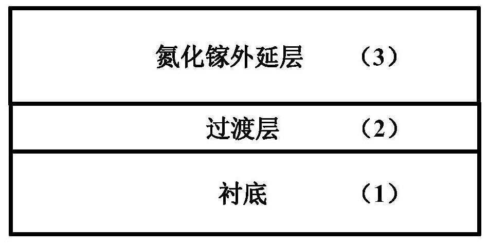
The invention discloses a gallium polar surface gallium nitride material and a homoepitaxial growth method, and mainly solves the problems of high dislocation density, poor surface appearance, high background carrier concentration, high growth process control difficulty and poor consistency of an existing gallium polar surface gallium nitride material. The gallium polar surface gallium nitride material structure comprises a substrate (1), a transition layer (2) and a gallium nitride epitaxial layer (3) from bottom to top, wherein the transition layer adopts InAlN or ScAlN or YAlN, and the substrate adopts a gallium polarity c surface gallium nitride single crystal substrate. The manufacturing method comprises the following steps of: growing the transition layer with the thickness of 1-10 nm on the substrate by using a molecular beam epitaxy method; and keeping the temperature of a reaction chamber, a nitrogen flow and nitrogen radio frequency source power unchanged, and growing the gallium nitride epitaxial layer on the transition layer. The gallium polar surface gallium nitride material is high in crystallization quality, smooth in surface appearance, low in background carrier concentration, simple in growth process and high in consistency, and can be used for manufacturing high-frequency microwave power devices and high-speed power electronic switching devices.

Description

technical field [0001] The invention belongs to the field of semiconductor material growth, and in particular relates to a gallium nitride semiconductor material on a gallium polar surface, which can be used for making high-frequency microwave power devices and high-speed power electronic switching devices. Background technique [0002] As a typical representative of the third-generation wide-bandgap semiconductor materials, gallium nitride materials have excellent properties such as wide bandgap, high saturation electron velocity, high breakdown field strength, high thermal conductivity, and radiation resistance. They are used in high-frequency microwave power devices. And high-speed power electronic switching devices have application potential. The heterojunction formed by gallium nitride material and InAlGaN material with wider bandgap has a two-dimensional electron gas with high carrier density and high mobility at its interface, which is the basic material structure of ...

Claims


Application Information

Patent Timeline
Patent Type & Authority Applications(China)
IPC IPC(8): H01L21/02H01L29/20H01L29/778
CPCH01L21/02389H01L21/02433H01L21/02458H01L21/0254H01L21/02631H01L29/2003H01L29/778
Inventor 薛军帅杨雪妍李蓝星姚佳佳孙志鹏张赫朋刘芳张进成郝跃
Owner XIDIAN UNIV
Learn More