Photoetching overlay mark and preparation method thereof

A lithography overlay and marking technology, which is applied in the field of lithography overlay marks and their preparation, can solve the problem of increasing the reject rate and production cost of power semiconductor devices, reducing the manufacturing process accuracy of power semiconductor devices, and the wear of lithography overlay marks, etc. problem, to achieve the effect of convenient metal peeling, clear metal marking points, clear and smooth contour lines

Active Publication Date: 2021-03-26
HEYUAN CHOICORE PHOTOELECTRIC TECH CO LTD
View PDF8 Cites 3 Cited by
  • Summary
  • Abstract
  • Description
  • Claims
  • Application Information

AI Technical Summary

Problems solved by technology

During this process, due to the physical bombardment of ions and the chemical reaction during annealing, the photolithographic overlay mark is worn, and the size of the alignment mark will change, the resolution of the pattern will decrease, the step difference will decrease, the contrast will decrease, and the pattern will be smoked. Disappearance and other issues
This affects the photolithographic alignment of the photolithographic overlay marks, reduces the precision of the subsequent manufacturing process of power semiconductor devices, and increases the reject rate and production cost of power semiconductor devices

Method used


Image

  • Photoetching overlay mark and preparation method thereof
  • Photoetching overlay mark and preparation method thereof
  • Photoetching overlay mark and preparation method thereof

Examples


Embodiment 1

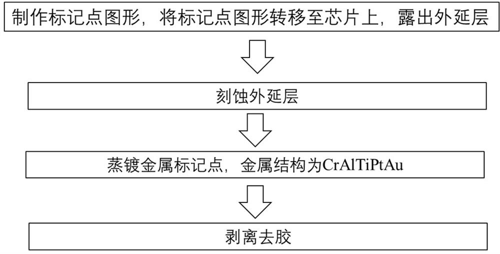
[0038] A photolithographic overlay mark is prepared by the following method:

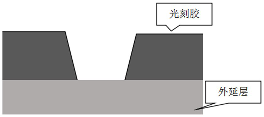
[0039] Step S1: Make a mark point pattern, the mark point pattern is the word "back"; transfer the mark point pattern to the chip by means of uniform glue, exposure, and development to expose the epitaxial layer; use positive photoresist for glue uniformity, and the thickness of the glue is 4μm;

[0040] Step S2: Etching the epitaxial layer; using inductively coupled plasma etching to etch the epitaxial layer, the etching gas is Cl 2 and BCl 3 , the etching depth is 8000A, and the etching angle is 80°;

[0041] Step S3: Evaporate metal marking points, the metal structure is CrAlTiPtAu; the thickness of the first layer of the metal structure is 50A; the thickness of the second layer of Al is 3000A; the thickness of the third layer of Ti is 2000A; the thickness of the fourth layer of Pt is 500A; the thickness of the fifth layer of Au 1000A.

[0042] Step S4: stripping and degumming; after soaking ...

Embodiment 2

[0044] A photolithographic overlay mark is prepared by the following method:

[0045] Step S1: Make a mark point pattern, the mark point pattern is "ten"; transfer the mark point pattern to the chip by means of uniform glue, exposure, and development to expose the epitaxial layer; use positive photoresist for glue uniformity, and the thickness of the glue is 3μm;

[0046] Step S2: Etching the epitaxial layer; using inductively coupled plasma etching to etch the epitaxial layer, the etching gas is Cl 2 and BCl 3 , the etching depth is 6000A, and the etching angle is 70°;

[0047] Step S3: Evaporate metal marking points, the metal structure is CrAlTiPtAu; the thickness of the first Cr layer of the metal structure is 20A; the thickness of the second Al layer is 1000A; the thickness of the third Ti layer is 500A; the thickness of the fourth Pt layer is 200A. The thickness of the fifth layer of Au is 3000A.

[0048] Step S4: stripping and degumming; after soaking in acetone for...


PUM

PropertyMeasurementUnit
Etching depthaaaaaaaaaa

Abstract

The invention relates to the technical field of semiconductors, in particular to a photoetching overlay mark and a preparation method thereof. The preparation method comprises the following steps of S1, manufacturing a mark point pattern, transferring the mark point pattern to a chip, and exposing an epitaxial layer; s2, etching the epitaxial layer; s3, evaporating a metal mark point, wherein themetal structure is CrAlTiPtAu, and the CrAlTiPtAu metal structure sequentially comprises a metal Cr layer, an Al layer, a Ti layer, a Pt layer and an Au layer from bottom to top. and S4, stripping anddegumming. The photoetching overlay mark prepared by the method provided by the invention has strong wear resistance and high resolution, is not easy to corrode, and is slightly influenced by the physical bombardment of ions and the corrosion of a chemical solution; and meanwhile, metal marking points can reflect light rays, so that the metal marking points are clearer, and the alignment accuracyis improved.

Description

technical field [0001] The invention relates to the technical field of semiconductors, in particular to a photolithographic overlay mark and a preparation method thereof. Background technique [0002] A semiconductor refers to a material whose conductivity at room temperature is between that of a conductor and an insulator. With the advancement of science and technology and the development of society, semiconductors are widely used in many fields such as integrated circuits, consumer electronics, communication systems, photovoltaic power generation, lighting, and high-power power conversion. The core units of most electronic products, such as computers, mobile phones or digital recorders, are closely related to semiconductors. In the semiconductor manufacturing process, photolithography is the core technology, and the accuracy of overlay will directly affect the appearance and performance of the product. [0003] The traditional overlay process forms power semiconductor de...

Claims


Application Information

Patent Timeline
IPC IPC(8): H01L23/544
CPCH01L23/544
Inventor 李国强
Owner HEYUAN CHOICORE PHOTOELECTRIC TECH CO LTD
Why Eureka
Try Eureka