Vertical cavity surface emitting semiconductor laser with upper and lower electrodes arranged in staggered manner

A technology of vertical cavity surface emission and lasers, which is applied in the direction of semiconductor lasers, lasers, laser components, etc., can solve the problems of long current path, reduced luminous efficiency of devices, large series resistance, etc., and achieves increased orbital angular momentum and luminous efficiency. The effect of increasing and decreasing the series resistance

Active Publication Date: 2021-03-12
CHANGCHUN UNIV OF SCI & TECH
View PDF13 Cites 0 Cited by
  • Summary
  • Abstract
  • Description
  • Claims
  • Application Information

AI Technical Summary

Problems solved by technology

For example, the upper and lower electrodes are only made in local areas in the upper and lower diagonal directions of the device, and the current bypasses the high-resistance region 9 between the upper and lower electrodes. It can be seen from this that although the current injection that occurs in the active gain region produces a rotational injection effect, but, The current injection is not uniform everywhere in the active gain region, the light intensity of each part of the beam of the emitted vortex hollow light is not uniform, and the beam quality is not high
For another example, because the current needs to flow diagonally along the up and down direction, it has to go around the high-resistance area 9, and the current path is long; viewed from the lateral direction, the lateral distance w between the upper and lower electrodes is relatively large, as figure 2 As shown, the horizontal resistance accounts for a large proportion of the series resistance. Therefore, the series resistance of this scheme is large, the heat generation becomes serious, and the luminous efficiency of the device decreases.

Method used


Image

  • Vertical cavity surface emitting semiconductor laser with upper and lower electrodes arranged in staggered manner
  • Vertical cavity surface emitting semiconductor laser with upper and lower electrodes arranged in staggered manner
  • Vertical cavity surface emitting semiconductor laser with upper and lower electrodes arranged in staggered manner

Examples


Embodiment Construction

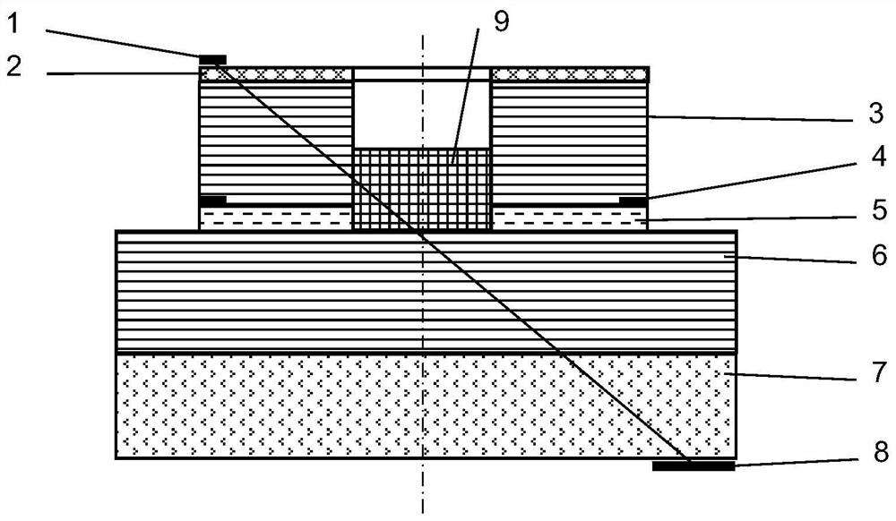
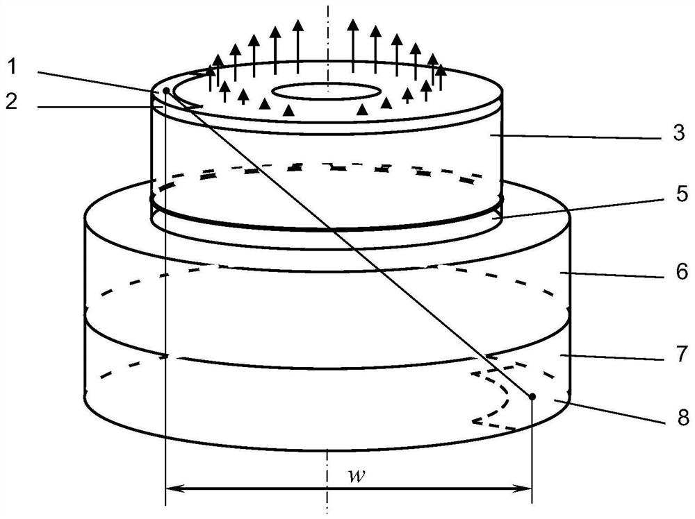
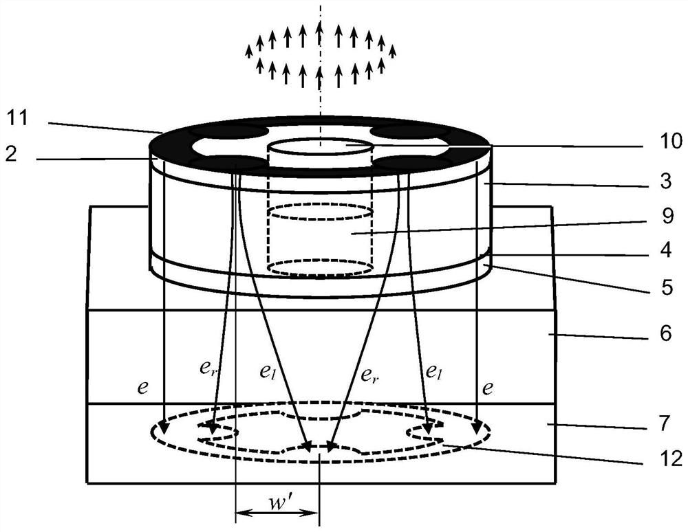
[0011] In the vertical cavity surface emitting semiconductor laser with disclination arrangement of the upper and lower electrodes of the present invention, the number of the extensions 14 of the disclination upper electrode 11 and the disclination lower electrode 12 is 3 or 4, and the disclination upper electrode 11 or the disclination The specific structure of the lower electrode 12 includes the following four types: 4 extensions 14 are located on the inner circle of the main body 13, such as Figure 4 Shown; 3 expansion parts 14 are located on the outer circle of main body part 13, as Figure 5 Shown; 3 expansion parts 14 are located on the inner circle of the main body part 13, as Figure 6 Shown; 4 expansion parts 14 are located on the outer circle of main body part 13, as Figure 7 shown. When the number of extensions 14 is 4, they are distributed at intervals of 1 / 2π radian, and the disclination upper electrode 11 and the disclination lower electrode 12 are disclinate...


PUM


Abstract

The invention relates to a vertical-cavity surface-emitting semiconductor laser with upper and lower electrodes arranged in a staggered manner and belongs to the technical field of semiconductor lasers. Current injection uniformity of an existing device is poor, and series resistance of the device is large. The laser is characterized in that a dislocation upper electrode is located on the upper surface of an ohmic contact layer, a dislocation lower electrode is located on the lower surface of a substrate, main body parts of the dislocation upper electrode and the dislocation lower electrode are annular, and the geometric center of the annular shape coincides with one point on the axis of the laser; expansion parts which are the same in shape and number are distributed along the outer circle or the inner circle of the annular body part at equal radian intervals, and the dislocation upper electrode and the dislocation lower electrode are arranged in the circumferential direction of the annular body part in a dislocated mode by one half of the radian. By improving the current injection uniformity of the device and reducing the series resistance of the device, the light intensity uniformity of the emitted vortex hollow light is improved, the heating of the device is reduced, and the luminous efficiency is improved.

Description

technical field [0001] The invention relates to a vertical-cavity surface-emitting semiconductor laser with discrepancy arrangement of upper and lower electrodes, belonging to the technical field of semiconductor lasers. Background technique [0002] Vortex light is a light beam with a spiral phase wavefront and a phase singularity. During the propagation process, the wavefront will take the propagation direction as the axis and propagate in a helical manner. The orbital angular momentum and dark hollow characteristics of the vortex light field can be used to capture, control and rotate microscopic particles with vortex light in optical micromanipulation, and use vortex light to store data, encode, decode, record and transmit information, and measure objects small deformation. However, the area where the light intensity is zero at the center of the vortex hollow light is larger, and its dark hollow characteristic is stronger. In addition to the use of vortex light, the vor...

Claims


Application Information

Patent Timeline
IPC IPC(8): H01S5/183
CPCH01S5/18322H01S5/18325
Inventor 晏长岭逄超杨静航岳云震冯源李辉郝永芹钱冉
Owner CHANGCHUN UNIV OF SCI & TECH
Why Eureka
Try Eureka