Novel MEMS high-Q-value non-solenoid integrated inductor and preparation method thereof

A technology integrating inductors and solenoids, applied in the field of microelectronics, can solve problems such as difficulty, high process cost, and subsequent packaging difficulties, and achieve the effects of suppressing substrate loss, reducing ohmic loss, and suppressing eddy current effects

Active Publication Date: 2021-02-23
FUDAN UNIV
View PDF4 Cites 1 Cited by
  • Summary
  • Abstract
  • Description
  • Claims
  • Application Information

AI Technical Summary

Problems solved by technology

[0007] However, the above-mentioned methods have various problems such as process complexity, inconvenient IC compatible integration, difficulty in subsequent packaging, insufficient mechanical stability, high process cost and difficulty, etc.

Method used


Image

  • Novel MEMS high-Q-value non-solenoid integrated inductor and preparation method thereof
  • Novel MEMS high-Q-value non-solenoid integrated inductor and preparation method thereof
  • Novel MEMS high-Q-value non-solenoid integrated inductor and preparation method thereof

Examples


Embodiment

[0062] The specific preparation process of a new type of MEMS high-Q non-solenoid integrated inductor is as follows:

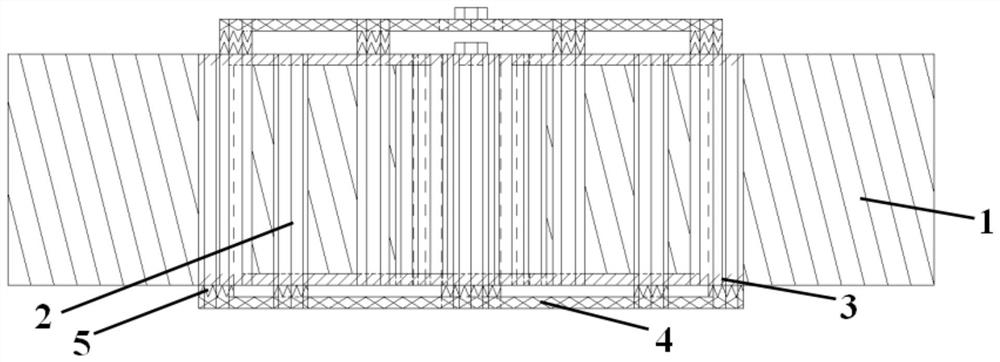
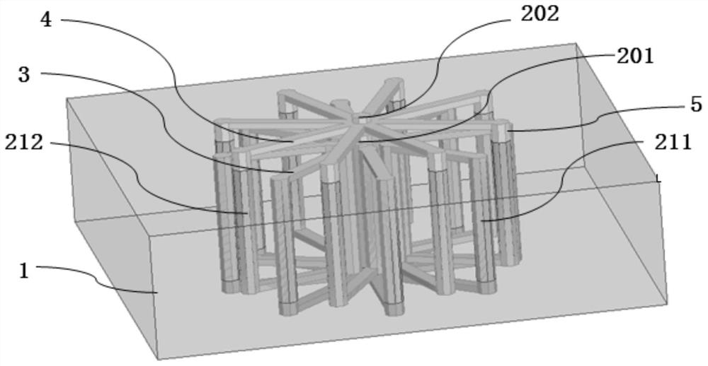
[0063] S1, such as Figure 3a As shown, a photoresist 6 is coated on a 4-inch silicon wafer (silicon substrate 1), prebaked, exposed, developed, and hardened. 2 The deep reactive ion etching (DRIE) process of the plasma low-temperature etching method of the reactive gas forms a TSV through hole with a smooth and steep side wall of 100 μm deep and a radius of 7.5 μm regular octagonal column on the silicon wafer. SiH based on sidewall 4 / O 2 The gas uses Low Pressure Chemical Vapor Deposition (LPCVD) to deposit a layer of 1 μm thick low-temperature oxide (LTO), which is used to isolate the inductor coil and the silicon base and reduce substrate loss. So far, a TSV via hole pattern with the number of inner TSV micro vias: the number of outer TSV micro vias=8:2*8 is formed. Among them, the inner TSV micro-vias correspond to the inner micro-copper column group ...


PUM

PropertyMeasurementUnit
thicknessaaaaaaaaaa

Abstract

The invention discloses a novel MEMS high-Q-value non-solenoid integrated inductor and a preparation method thereof. The integrated inductor comprises a silicon substrate; TSV micro-copper columns embedded in the silicon substrate, wherein the two ends of each TSV micro-copper column are exposed, and each TSV micro-copper column comprises a central port copper column, an inner side micro-copper column set, a first outer side micro-copper column set and a second outer side micro-copper column set; a first surface layer interconnection coil including a top surface layer interconnection coil anda bottom surface layer interconnection coil; an outer surface layer interconnection copper column; and a second surface layer interconnection coil including a top outer surface layer interconnection coil and a bottom outer surface layer interconnection coil. According to the invention, an improved embedded non-solenoid integration scheme is adopted, the inductor and the silicon substrate are isolated through the low-temperature oxide layer, the substrate loss is reduced, the non-solenoid structure surface layer interconnection coils are supported through the insulating material, and the multi-turn coil is embedded and integrated in a small area. Finally, the miniature integrated inductor which is low in loss, small in stray parasitic capacitance and high in Q value is formed, and meanwhilethe miniature integrated inductor is compatible with the packaging process and stable in machinery.

Description

technical field [0001] The invention relates to integrated passive components in the field of microelectronic technology, in particular to a novel MEMS high-Q value non-solenoid integrated inductor with a peak quality factor Q reaching 40. Background technique [0002] In the past 30 years, with the development of electronic communication technology and the increasing functions of handheld devices such as smart consumer electronics, inductors, as basic and necessary electronic components, are widely used in integrated circuits, such as matching networks, filters, low-noise amplifiers , Transceivers, Voltage Controlled Oscillators, etc. Due to the constraints of packaging cost, size and performance conditions, traditional discrete inductors no longer meet the urgent needs of small size and low power consumption of integrated circuits. The demand for inductors with low energy consumption, small size, low noise, and high frequency bands continues Increase. The quality factor ...

Claims


Application Information

Patent Timeline
Patent Type & Authority Applications(China)
IPC IPC(8): H01F27/28H01F27/30H01F41/00H01F41/18H01F41/22
CPCH01F41/00H01F41/18H01F41/22H01F27/2866H01F27/2871H01F27/303
Inventor 周盛锐徐玲杨颖琳
Owner FUDAN UNIV
Why Eureka
Try Eureka