Method for reducing dislocation and stress by using layer dislocation, LED epitaxial wafer and application
A technology of LED epitaxial wafers and dislocations, which is applied in semiconductor devices, electrical components, circuits, etc., can solve the problems of reduced overlapping integrals of electron and hole wave functions, reduced probability of radiation recombination, etc., to reduce dislocation density and residual stress , Make up for the effect of lattice constant mismatch
- Summary
- Abstract
- Description
- Claims
- Application Information
AI Technical Summary
Problems solved by technology
Method used
Image
Examples
Embodiment 1
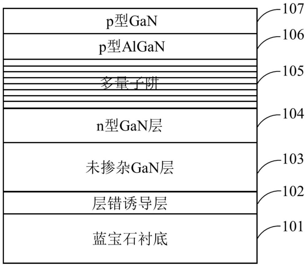
[0035] 1) Select the c-plane sapphire substrate, put it into the magnetron sputtering reaction chamber, the target material is high-purity Al, the reaction gas is nitrogen, the carrier gas is argon, and the AlN deposition thickness is 25nm;
[0036] 2) Put it into the MOCVD reaction chamber, pass through ammonia gas and trimethylgallium, and grow GaN with a thickness of 15nm at 800°C;
[0037] 3) Pass in hydrogen and ammonia, and heat up to 1150°C;
[0038] 4) growing a 3 μm thick undoped GaN layer on the stacking fault induction layer;
[0039] 5) Lower the temperature to 1100°C, and grow a 2 μm thick n-type GaN layer on the undoped GaN;
[0040] 6) Grow 9 periods of multi-quantum well layers on n-type GaN, GaN barrier layer: thickness is 15nm, growth temperature is 850°C, InGaN well layer: thickness is 3nm, growth temperature is 700°C;
[0041] 7) heating up to 950°C, and growing a 30nm-thick p-type AlGaN layer on the multiple quantum wells;
[0042] 8) Regrowing a p-type...
Embodiment 2
[0045] 1) Select the c-plane sapphire substrate, put it into the magnetron sputtering reaction chamber, the target material is high-purity Al, the reaction gas is nitrogen, the carrier gas is argon, and the AlN deposition thickness is 20nm;
[0046] 2) Put it into the MOCVD reaction chamber, pass through ammonia gas, trimethylgallium and trimethylaluminum, and grow 10nm thick Al at 900°C 0.2 Ga 0.8 N;
[0047] 3) Pass in hydrogen and ammonia, and heat up to 1150°C;
[0048] 4) Introducing ammonia gas and trimethylgallium to grow a 3 μm thick undoped GaN layer;
[0049] 5) Lower the temperature to 1100°C, and grow a 2.5 μm thick n-type GaN layer on the undoped GaN;
[0050] 6) Grow 8 periods of multiple quantum well layers on n-type GaN, GaN barrier layer: thickness is 13.5nm, growth temperature is 850°C, InGaN well layer: thickness is 3.5nm, growth temperature is 700°C;
[0051] 7) heating up to 950°C, and growing a 30nm-thick p-type AlGaN layer on the multiple quantum wel...
PUM
| Property | Measurement | Unit |
|---|---|---|
| thickness | aaaaa | aaaaa |
| thickness | aaaaa | aaaaa |
| thickness | aaaaa | aaaaa |
Abstract
Description
Claims
Application Information
 - R&D Engineer
- R&D Manager
- IP Professional
- Industry Leading Data Capabilities
- Powerful AI technology
- Patent DNA Extraction
Browse by: Latest US Patents, China's latest patents, Technical Efficacy Thesaurus, Application Domain, Technology Topic, Popular Technical Reports.
© 2024 PatSnap. All rights reserved.Legal|Privacy policy|Modern Slavery Act Transparency Statement|Sitemap|About US| Contact US: help@patsnap.com


