Light and safe conductive film and preparation method thereof
A conductive thin film, safe technology, applied in the direction of resistance manufacturing, resistors with positive temperature coefficients, circuits, etc., can solve the problems of slow heat transfer, non-response, etc., to reduce the amount of metal used, not easy to separate the conductive layer, and strengthen the combination force effect
- Summary
- Abstract
- Description
- Claims
- Application Information
AI Technical Summary
Problems solved by technology
Method used
Image
Examples
Embodiment 1
[0033] Conductive films were prepared by the following steps:
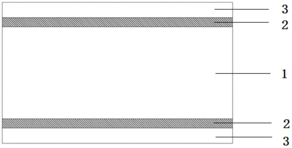
[0034] Step 1: uniformly mix polyvinylidene fluoride (PVDF) with a mass fraction of 70% and 30% conductive carbon nanotubes, heat, melt and stir evenly, and stretch to form a PTC matrix layer with a thickness of 6 μm after tape casting;
[0035] Step 2: Wind the PTC matrix layer on the drum, and place the drum equipment in a vacuum environment with a vacuum degree of ≤10 -3 Pa;
[0036] Step 3: Treating the PTC base layer material with plasma treatment of a mixed gas of oxygen and argon;
[0037] Step 4: In the vacuum environment, the aluminum-zinc alloy (80% aluminum, 20% zinc) is subjected to resistance heating, melting and evaporation to obtain gaseous metal, which is deposited on the PTC substrate layer to form a 50nm aluminum-zinc alloy reinforcement layer;
[0038] Step 5: Continue to melt and evaporate aluminum on the surface of the aluminum-zinc alloy reinforcement layer by means of resistance heating. T...
Embodiment 2
[0043] Conductive films were prepared by the following steps:
[0044] Step 1: uniformly mix polypropylene (PP) with a mass fraction ratio of 60% and 40% graphite, heat, melt and stir evenly, form a sheet by co-extrusion and then stretch to form a PTC matrix layer with a thickness of 6 μm;
[0045] Step 2: Wind the PTC matrix layer on the drum, and place the drum equipment in a vacuum environment with a vacuum degree of ≤10 -3 Pa;
[0046] Step 3: treating the PTC matrix layer material with nitrogen ions by ion implantation;
[0047] Step 4: In the vacuum environment, perform magnetron sputtering on the nickel target, and sputter a layer of 500nm metal nickel enhancement layer on the PTC substrate layer;
[0048] Step 5: Continue to deposit copper on the surface of the metal nickel reinforcement layer by magnetron sputtering. The deposited copper touches the metal nickel reinforcement layer to form a thin copper metal conductive layer, and the roller rolls back and forth wit...
Embodiment 3
[0053] Conductive films were prepared by the following steps:
[0054] Step 1: uniformly mix polyimide (PI) with a mass fraction ratio of 70% and 30% Ni powder, heat, melt and stir evenly, and stretch to form a PTC matrix layer with a thickness of 4.5 μm after tape casting;
[0055] Step 2: Take the polymer conductive composite material with positive temperature sensitive (PTC) effect as the matrix layer, wind it on the drum, and place the drum equipment in a vacuum environment, with a vacuum degree of ≤10 -3 Pa;
[0056] Step 3: Treating the PTC base layer material with plasma treatment of a mixed gas of oxygen and argon;
[0057] Step 4: In the vacuum environment, the metal tin is melted by resistance heating, and a layer of 200nm metal tin intermediate layer is evaporated on the PTC base layer;
[0058] Step 5: Melt and evaporate the copper-nickel alloy on the surface of the metal tin reinforcement layer by means of electron beam heating. The gaseous copper-nickel alloy c...
PUM
| Property | Measurement | Unit |
|---|---|---|
| thickness | aaaaa | aaaaa |
| thickness | aaaaa | aaaaa |
| thickness | aaaaa | aaaaa |
Abstract
Description
Claims
Application Information
 - R&D
- Intellectual Property
- Life Sciences
- Materials
- Tech Scout
- Unparalleled Data Quality
- Higher Quality Content
- 60% Fewer Hallucinations
Browse by: Latest US Patents, China's latest patents, Technical Efficacy Thesaurus, Application Domain, Technology Topic, Popular Technical Reports.
© 2025 PatSnap. All rights reserved.Legal|Privacy policy|Modern Slavery Act Transparency Statement|Sitemap|About US| Contact US: help@patsnap.com

