Embedding and packaging structure for organic substrate integrated with antenna and radio frequency front end

A radio frequency front-end, packaging structure technology, applied in the direction of semiconductor/solid-state device components, semiconductor devices, electrical components, etc., can solve problems such as electromagnetic interference, limit antenna performance, and metal heat sink heat dissipation methods are no longer applicable, and improve antenna performance. Bandwidth, effect of reducing parasitics and transmission loss

Active Publication Date: 2020-12-11
INST OF MICROELECTRONICS CHINESE ACAD OF SCI
View PDF5 Cites 0 Cited by
  • Summary
  • Abstract
  • Description
  • Claims
  • Application Information

AI Technical Summary

Problems solved by technology

[0004] The integration of the antenna and the RF front-end mainly faces the following technical problems: Most of the millimeter-wave chips used in the RF front-end are based on the compound semiconductor process, and the metal grounding requirements on the back limit the packaging form of the chip to wire bonding. However, as the operating frequency increases, the bond The parasitic effect of the bonding wire is becoming more and more obvious; at the same time, the demand for thinner and smaller packages of electronic products is constantly increasing, but the thinner and lighter package structure limits the thickness of the antenna base, thereby limiting the improvement of the antenna performance; in addition, the antenna and radio frequency When the front-end is integrated, the problem of electromagnetic interference between the active chip and the active chip, and between the antenna and the active chip is particularly serious; moreover, after the antenna is integrated with the RF front-end, the heat dissipation method of mounting a metal heat sink on the package is no longer Be applicable

Method used


Image

  • Embedding and packaging structure for organic substrate integrated with antenna and radio frequency front end
  • Embedding and packaging structure for organic substrate integrated with antenna and radio frequency front end
  • Embedding and packaging structure for organic substrate integrated with antenna and radio frequency front end

Examples


Embodiment Construction

[0048] In order to make the object, technical solution and advantages of the present invention clearer, the present invention will be further described in detail below in conjunction with specific embodiments and with reference to the accompanying drawings.

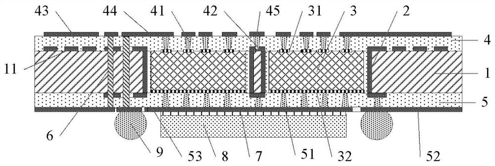
[0049] In the present invention, "disposed on" or "attached to" is used to include a direct contact relationship with a single or multiple components. For example, the No. 2 dielectric layer is arranged on the lower surface of the core board, which means that the No. 2 dielectric layer is in direct contact with the core board, that is, the No. 2 dielectric layer is in direct contact with the lower surface of the core board. Moreover, the ordinal numbers used in the specification and claims, such as "first", "second", "number one" or "number two", are used to modify the components claimed for protection, which do not themselves contain and represent the Parts have any previous ordinal numbers, nor do they imply the order o...


PUM


Abstract

An embedding and packaging structure for organic substrate integrated with antenna and radio frequency front end comprises a radio frequency front end module, two dielectric layers and an antenna module. The radio frequency front end module comprises a core plate, wherein the interior of the core plate comprises at least one through groove; at least one active chip which is buried in the through groove of the core plate; two dielectric layers which are respectively a first dielectric layer and a second dielectric layer, wherein the first dielectric layer is arranged on the upper surface of thecore plate and is provided with a plurality of first metallized blind holes in a penetrating manner, and the second dielectric layer is arranged on the lower surface of the core plate and is providedwith a plurality of second metallized blind holes in a penetrating manner. A plurality of metallized through holes are formed in the first dielectric layer, the core plate and the second dielectric layer in a penetrating manner. The antenna module comprises at least one antenna unit arranged on the upper surface of the first dielectric layer; a periodic metal structure which is arranged on the upper surface of the core plate; a metal ground plane which is arranged on the lower surface of the second dielectric layer, wherein the metal ground plane and the periodic metal structure jointly serveas an antenna reflection plane.

Description

technical field [0001] The invention relates to the technical field of semiconductor packaging, in particular to an organic substrate embedded packaging structure integrating a millimeter wave antenna and a radio frequency front end. Background technique [0002] In order to improve the integration level, the International Semiconductor Technology Development Route Organization proposed Beyond Moore's Law, aiming to integrate processors, memories, radio frequency modules, digital modules, analog modules, optoelectronic modules, sensor modules, etc. into a single package to achieve system-in-package (System in Package, SiP), if the antenna is also integrated in the system-in-package, it is called antenna-level packaging (Antenna in Pakcage, AiP). [0003] Among them, SiP covers integrated solutions from traditional 2D modules including multiple active chips and passive components to more complex modules such as PiP, PoP, 2.5D and 3D. The substrate materials used include LTCC,...

Claims


Application Information

Patent Timeline
IPC IPC(8): H01L23/31H01L25/16H01L23/66H01L23/36
CPCH01L23/31H01L25/16H01L23/66H01L23/36H01L2223/6683
Inventor 王启东薛梅曹立强方志丹
Owner INST OF MICROELECTRONICS CHINESE ACAD OF SCI
Why Eureka
Try Eureka