Single-step rapid preparation method of porous silicon-gold dendritic crystal composite structure
A composite structure and porous silicon technology, applied in nanotechnology, nanotechnology, instruments, etc. for sensing, can solve problems such as high environmental requirements, complicated operation, and long preparation time, and achieve simple steps, more steps to solve, The effect of efficient preparation
- Summary
- Abstract
- Description
- Claims
- Application Information
AI Technical Summary
Problems solved by technology
Method used
Image

Examples
Embodiment 1
[0031] A single-step rapid preparation method for a porous silicon-gold dendrite composite structure, comprising the following steps:
[0032] (1) Pretreatment: select a P-type silicon chip, preferably, the silicon chip is a [100] crystal orientation P-type single crystal silicon, the resistivity is 10-20Ω·cm, and the thickness is 525 μm, and the silicon chip is cut with a diamond tool Divide into square silicon wafers of 1.5cm×1.5cm; place the cut square silicon wafers in a beaker filled with deionized water, alcohol, and acetone in turn and perform ultrasonic cleaning for 10 minutes to remove oil and impurities on the square silicon wafers , and then blow dry with a nitrogen gun;
[0033] (2) Preparation of electrochemical corrosion solution: use suction pipe to take out 16mL of HF (48wt%), 9mL of DMF (analytical pure AR) and 8mL of tetrachloroauric acid solution respectively on the operating table with fume hood and put into plastic measuring cylinder An electrochemical co...
Embodiment 2
[0039] The preparation steps of the porous silicon-gold dendrite composite structure are the same as in Example 1, the difference is that the concentration of tetrachloroauric acid solution is adjusted to 0.2M;
[0040] SEM characterization and SERS performance analysis of porous silicon-gold dendrite composite structure:
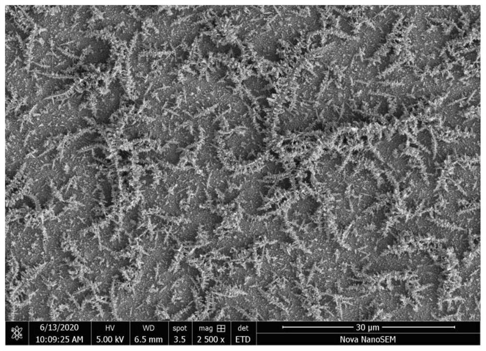
[0041] image 3 It is the SEM image of the porous silicon-gold dendrite composite structure prepared in Example 2, showing the structure under this corrosion condition, and it can be seen that a large number of gold nanodendrites are attached to the porous silicon.
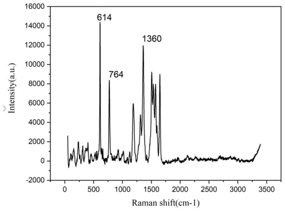
[0042] Figure 4 It is the Raman spectrogram of porous silicon-gold dendrite composite structure and pure porous silicon, and the concentration of R6G is 10 in embodiment 2 -6 M, at 614cm -1 , 764cm -1 , 1360cm -1 , 1502cm -1 and 1643cm -1 It can be clearly seen that the spectral characteristic peaks of R6G and their peaks have been greatly enhanced, and the SERS intensity has been great...
Embodiment 3
[0044]The preparation steps of the porous silicon-gold dendrite composite structure are the same as in Example 1, the difference being that the concentration of tetrachloroauric acid solution is adjusted to 0.5M;
[0045] Porous silicon-gold dendrite composite structure SEM characterization and SERS performance analysis:
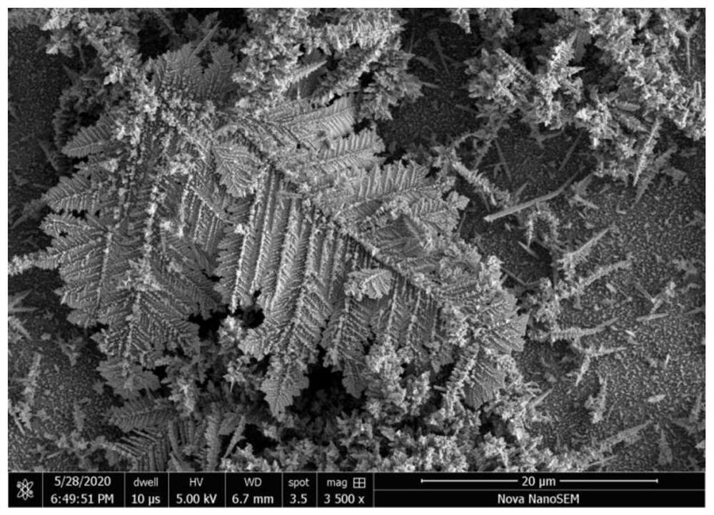
[0046] Through the SEM morphology test of the experimental samples; Figure 5 It is the SEM picture of the porous silicon-gold dendrite composite structure prepared in Example 3, showing the structure under this corrosion condition. It can be seen that denser gold nanodendrites are attached to the porous silicon.
[0047] Figure 6 is the Raman spectrum of porous silicon-gold dendrite composite structure and pure porous silicon, the concentration of R6G in this experiment is 10 -6 M, at 614cm -1 , 764cm -1 , 1360cm -1 , 1502cm -1 and 1643cm -1 It can be clearly seen that the spectral characteristic peak of R6G and its peak intensity have decreased com...
PUM
| Property | Measurement | Unit |
|---|---|---|
| electrical resistivity | aaaaa | aaaaa |
| thickness | aaaaa | aaaaa |
Abstract
Description
Claims
Application Information
 - R&D
- Intellectual Property
- Life Sciences
- Materials
- Tech Scout
- Unparalleled Data Quality
- Higher Quality Content
- 60% Fewer Hallucinations
Browse by: Latest US Patents, China's latest patents, Technical Efficacy Thesaurus, Application Domain, Technology Topic, Popular Technical Reports.
© 2025 PatSnap. All rights reserved.Legal|Privacy policy|Modern Slavery Act Transparency Statement|Sitemap|About US| Contact US: help@patsnap.com