


Quick Research
Generate reliable direction feasibility study reports for your R&D in just a few steps.

Technical Q&A
Discover and master advanced knowledge NOW. Basics, ideas, possibilities, all at once.

Find Solutions
As an expert in R&D theories, this can generate solutions to your technical problems instantly.

Evaluate Feasibility
Analyze your overall solution with one click, know your potential R&D risks in advance.

Monitor Landscape
Get weekly tech updates, stay abreast of the latest tech innovations and key insights.
A method for preparing periodic pn junction graphene based on high-purity semi-insulating silicon carbide substrate
A silicon carbide substrate, semi-insulating technology, applied in the field of microelectronic materials, can solve the problems of reduced doping concentration, long atomic diffusion distance, unsuitable for pn junction strips, etc., to ensure integrity, improve transmission characteristics, and excellent Effects of photoelectric conversion characteristics and electrical transport properties
- Summary
- Abstract
- Description
- Claims
- Application Information
AI Technical Summary
Problems solved by technology
Method used
Image


Examples
preparation example Construction
[0048] The high-temperature furnace for preparing periodic pn-junction graphene in the present invention is prior art, and the high-temperature furnace used is a vertical high-temperature furnace generally sold on the market.
[0049] The high-purity hydrogen / argon used in the present invention is hydrogen / argon with a purity above 99.999%; the silicon carbide substrate used is a high-purity semi-insulating silicon carbide substrate with a purity above 99.999%.
Embodiment 1
[0051] (1) A 4-inch high-purity semi-insulating 4H-silicon carbide crystal is ground and polished to obtain a high-purity semi-insulating silicon carbide wafer substrate with a thickness of 350 μm, so that the surface roughness is below 0.5nm and the flatness is between 10μm, then clean the silicon surface and package it for use;
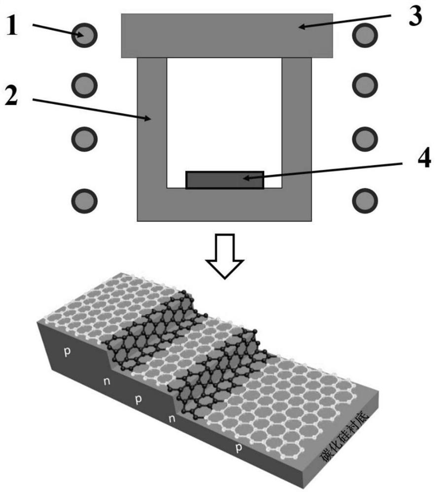
[0052] (2) Place the silicon carbide wafer substrate prepared in step (1) flat in the graphite crucible, with the silicon side facing up, and press the graphite cover tightly. Then placed in the medium frequency induction heating furnace chamber, the vacuum degree in the furnace chamber is 5.0×10 -5 mbar, quickly raise the temperature to 1300-1350°C, and keep it warm for 40 minutes to remove the adsorbed impurity gas. The specific placement is as follows figure 1 shown;
[0053] (3) Introduce high-purity hydrogen gas into the furnace chamber, control the pressure at 500mbar, continue to raise the temperature to 1550°C, and perform hydrogen etching...
Embodiment 2
[0058] (1) A 4-inch high-purity semi-insulating 4H-silicon carbide crystal is ground and polished to obtain a high-purity semi-insulating silicon carbide wafer substrate with a thickness of 350 μm, so that the surface roughness is below 0.5nm and the flatness is between 10μm, then clean the silicon surface and package it for use;
[0059] (2) Place the silicon carbide wafer substrate prepared in step (1) flat in the graphite crucible, with the silicon side facing up, and press the graphite cover tightly. Then placed in the medium frequency induction heating furnace chamber, the vacuum degree in the furnace chamber is 5.0×10 -5 mbar, quickly raise the temperature to 1300-1350°C, and keep it warm for 40 minutes to remove the adsorbed impurity gas. The specific placement is as follows figure 1 shown;
[0060] (3) Introduce high-purity hydrogen gas into the furnace chamber, control the pressure at 500mbar, continue to raise the temperature to 1550°C, and perform hydrogen etching...
PUM
| Property | Measurement | Unit |
|---|---|---|
| width | aaaaa | aaaaa |
Abstract
Description
Claims
Application Information
 - R&D Engineer
- R&D Manager
- IP Professional
- Industry Leading Data Capabilities
- Powerful AI technology
- Patent DNA Extraction
Browse by: Latest US Patents, China's latest patents, Technical Efficacy Thesaurus, Application Domain, Technology Topic, Popular Technical Reports.
© 2024 PatSnap. All rights reserved.Legal|Privacy policy|Modern Slavery Act Transparency Statement|Sitemap|About US| Contact US: help@patsnap.com