


Quick Research
Generate reliable direction feasibility study reports for your R&D in just a few steps.

Technical Q&A
Discover and master advanced knowledge NOW. Basics, ideas, possibilities, all at once.

Find Solutions
As an expert in R&D theories, this can generate solutions to your technical problems instantly.

Evaluate Feasibility
Analyze your overall solution with one click, know your potential R&D risks in advance.

Monitor Landscape
Get weekly tech updates, stay abreast of the latest tech innovations and key insights.
Amplifying circuit, photoelectric signal detection circuit, detection chip circuit and chip
A technology for amplifying circuits and photoelectric signals, applied in the direction of amplifiers, amplification control, amplifier combination, etc., can solve problems such as being easily interfered by ambient light and noise, difficult to adapt to the loop establishment time, and difficult to adapt to the lower limit cut-off frequency
- Summary
- Abstract
- Description
- Claims
- Application Information
AI Technical Summary
Problems solved by technology
Method used
Image

Examples
specific Embodiment 1
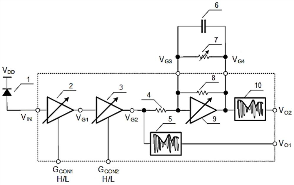
[0034] A kind of photoelectric signal detection circuit of the present invention, as figure 1 As shown, it includes an optical signal receiving circuit, a voltage conversion circuit, an amplifying circuit, and a detection circuit connected in sequence. The optical signal receiving circuit is used to convert the optical signal into a current signal. After the current signal passes through the voltage conversion circuit, it is converted into a voltage signal. The voltage signal is amplified, and the voltage amplitude signal is obtained after passing through the detection circuit.
[0035] The optical signal receiving circuit includes a photodiode 1, the cathode of the photodiode 1 is connected to the power supply terminal, and the anode is connected to the voltage conversion circuit. When the light signal irradiates the photodiode, a current is generated in the photodiode.
[0036] The voltage conversion circuit includes a transimpedance amplifier circuit 2 for converting curren...
specific Embodiment 2
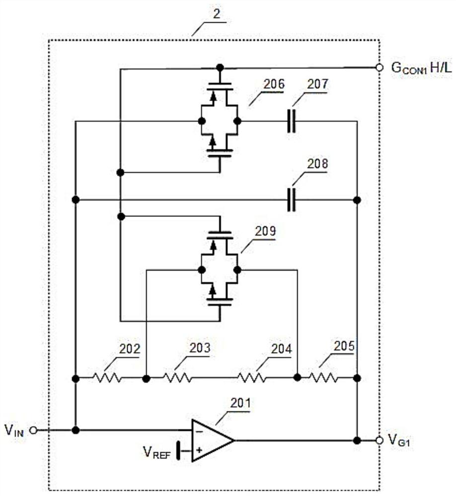
[0046] A transimpedance amplifier circuit in a photoelectric signal detection circuit of the present invention, such as figure 2 As shown, it includes a transimpedance operational amplifier 201 and a transimpedance RC circuit network. The transimpedance RC circuit network is connected in parallel between the negative input terminal and the output terminal of the transimpedance operational amplifier 201, and the positive input terminal of the transimpedance operational amplifier 201 is connected to the setting value VREF terminal.
[0047] The transimpedance RC circuit network comprises a transimpedance resistance circuit composed of four serially connected resistors 202, 203, 204, and 205, a first transimpedance capacitance circuit, a second transimpedance capacitance circuit, a transimpedance resistance circuit, a first transimpedance The resistance-capacitance circuit and the second transresistance-capacitance circuit are connected in parallel.
[0048] A first transimpeda...
specific Embodiment 3
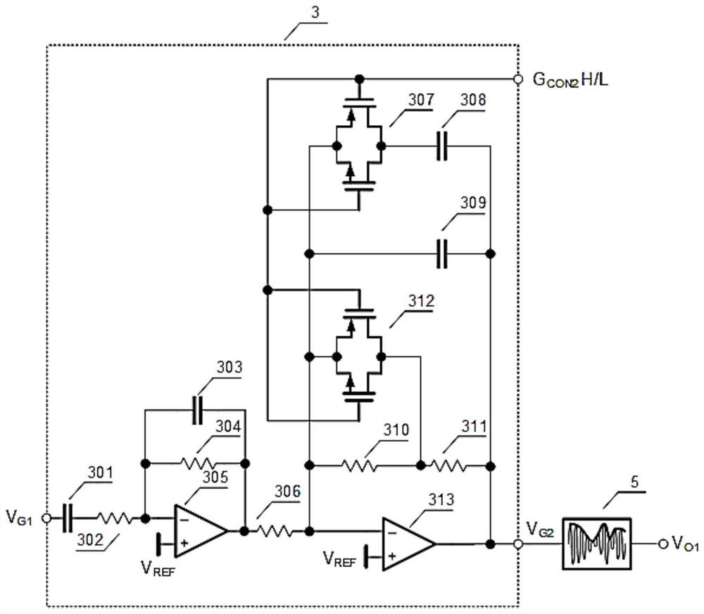
[0056] Amplifying circuit in a kind of photoelectric signal detection circuit of the present invention, as image 3 As shown, it includes a coupling capacitor 301 connected in sequence, and a second-stage op-amp sub-circuit. The first-stage op-amp sub-circuit is used to amplify with a fixed magnification, and the second-stage op-amp sub-circuit is used to amplify with an adjustable magnification. .
[0057] The coupling capacitor 301 is used to isolate the DC component of the signal, and transmit the AC component of the signal to the amplifying circuit for amplification.
[0058] The first-stage op-amp subcircuit includes a first op-amp amplifier 305 , a first op-amp RC circuit network, and a first input resistor 302 , and the first op-amp RC circuit network includes a resistor 304 and a capacitor 303 connected in parallel.
[0059] One end of the first input resistor 302 is connected to one end of the coupling capacitor 301, the other end is connected to the negative input t...
PUM
 Abstract
Description
Claims
Application Information
 - R&D Engineer
- R&D Manager
- IP Professional
- Industry Leading Data Capabilities
- Powerful AI technology
- Patent DNA Extraction
Browse by: Latest US Patents, China's latest patents, Technical Efficacy Thesaurus, Application Domain, Technology Topic, Popular Technical Reports.
© 2024 PatSnap. All rights reserved.Legal|Privacy policy|Modern Slavery Act Transparency Statement|Sitemap|About US| Contact US: help@patsnap.com