vdmosfet and its preparation method and semiconductor device

A conductive type, lightly doped technology, applied in semiconductor devices, semiconductor/solid-state device manufacturing, electrical components, etc., can solve problems such as low device withstand voltage, low interface state density, channel mobility, gate oxide breakdown, etc.

Active Publication Date: 2022-05-13
BYD CO LTD
View PDF4 Cites 0 Cited by
  • Summary
  • Abstract
  • Description
  • Claims
  • Application Information

AI Technical Summary

Problems solved by technology

There are following disadvantages in this lateral channel device structure: one is that there is a JFET region, which will increase the on-resistance of the device (i.e., the on-state loss during application), and the method for reducing the resistance of the JFET region in the related art is to increase the distance between pwells or It is N-implantation in the JFET area, but it is easy to cause short channel effect (the device is turned on in advance) and the carrier concentration under the gate oxide layer is relatively high, so that the gate oxide layer bears a large voltage, which will lead to early breakdown of the gate oxide. The withstand voltage of the device is reduced; the second is that the on-resistance of the device is inversely proportional to the withstand voltage value. If the on-resistance is reduced by increasing the concentration of the N-drift layer 20, a part of the withstand voltage of the device will be lost, and it is impossible to reduce the conduction resistance. The on-resistance ensures the withstand voltage of the device at the same time; the third is due to the existence of C element, SiC / SiO 2 The interface state density of the material is about three times that of Si, and the high interface state density leads to low channel mobility; the fourth is due to the higher SiC / SiO 2 Compared with the silicon device, the interface state density of the material and the gate oxide layer are easy to break down in advance, so that the actual withstand voltage value of the device is much lower than the calculated value
[0004] Therefore, the current VDMOSFET related technologies still need to be improved

Method used


Image

  • vdmosfet and its preparation method and semiconductor device
  • vdmosfet and its preparation method and semiconductor device
  • vdmosfet and its preparation method and semiconductor device

Examples


preparation example Construction

[0055] The method can quickly and effectively prepare and obtain the aforementioned VDMOSFET, has simple steps, is convenient to operate, and is easy to realize industrial production.

[0056] In yet another aspect of the present application, the present application provides a semiconductor device. According to an embodiment of the present application, the semiconductor device includes the aforementioned VDMOSFET. The semiconductor device includes all the features and advantages of the above-mentioned VDMOSFET, which will not be repeated here.

[0057] According to the embodiment of the present application, the specific type of the semiconductor device can be MOSFET (Metal-Oxide Semiconductor Field Effect Transistor), IGBT (Insulated Gate Bipolar Transistor), and those skilled in the art can understand that, in addition to the aforementioned In addition to the VDMOSFET, and including the necessary structures and components of conventional devices, details will not be repeated...

Embodiment 1

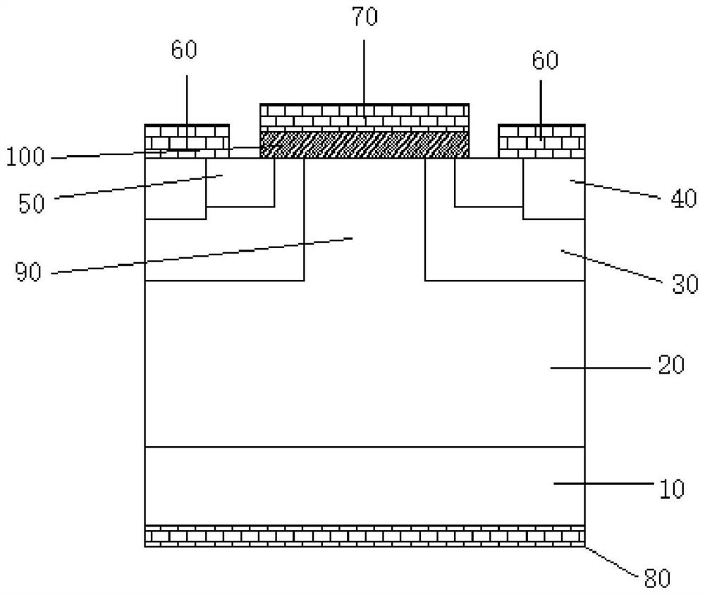
[0060] Step 1: Epitaxially form an N-type SIC doped layer 8 on a heavily doped N+ type SIC substrate 1 with a concentration of 1×10 15 cm -3 , the thickness is 10 microns, and the doping impurity is nitrogen (N);

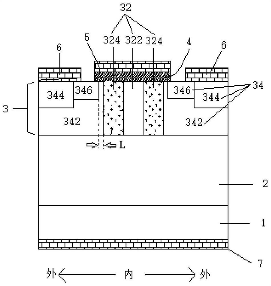
[0061] Step 2: Perform ion implantation on the N-type SIC doped layer 8 to form a P-well region and a P-doped region of a super junction structure, and the implantation concentration is 2×10 13 cm -3 , the doping impurity is aluminum (Al);

[0062] Step 3: Perform ion implantation on the N-type SIC doped layer 8 to form an N-doped region of a super junction structure, with an implantation concentration of 1.5×10 13 cm -3 ;

[0063] Step 4: Photolithography and implantation on the N-type SIC doped layer 8 to form a source region and a contact region; the doping concentration of the source region is 2×10 15 cm -3 , the doping concentration of the contact area is 1x10 16 cm -3 ; and carry out high temperature annealing after implantation, the annealing tempera...

Embodiment 2

[0068] Step 1: Epitaxially form an N-type SIC doped layer 8 on a heavily doped N+ type SIC substrate 1 with a concentration of 1×10 15 cm -3 , the thickness is 10 microns, and the doping impurity is nitrogen (N);

[0069] Step 2: Perform ion implantation on the N-type SIC doped layer 8 to form a P-well region and a P-doped region of a super junction structure, and the implantation concentration is 2×10 13 cm -3 , the doping impurity is aluminum (Al);

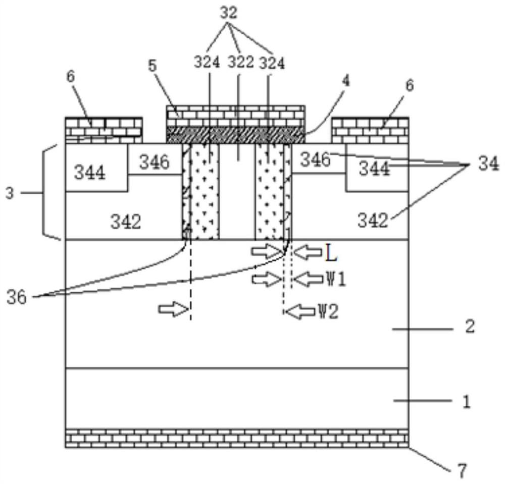
[0070] Step 3: Perform ion implantation on the N-type SIC doped layer 8 to form an N-doped region of a super junction structure, with an implantation concentration of 1.5×10 13 cm -3 ; The overlapping width with the P-well region is 0.5 microns respectively;

[0071] Step 4: Photolithography and implantation on the N-type SIC doped layer 8 to form a source region and a contact region; the doping concentration of the source region is 2×10 15 cm -3 , the doping concentration of the contact area is 1x10 16 cm -3 ; and perf...


PUM

PropertyMeasurementUnit
widthaaaaaaaaaa
lengthaaaaaaaaaa
widthaaaaaaaaaa

Abstract

The present application provides a VDMOSFET and its preparation method and a semiconductor device. The VDMOSFET includes a heavily doped substrate of the first conductivity type, a lightly doped drift layer of the first conductivity type, a lightly doped well region of the second conductivity type, a second conductivity type A heavily doped contact region, a heavily doped source region of the first conductivity type, a lightly doped region of the second conductivity type, a lightly doped region of the first conductivity type, a gate oxide layer, a gate, a source and a drain. The VDMOSFET introduces the lightly doped region of the second conductivity type and the lightly doped region of the first conductivity type to form alternating PN columns (super junction structure), which can greatly reduce the on-resistance without reducing the breakdown voltage. At the same time, it can effectively protect the gate oxide layer from being broken down and improve the reliability of the device.

Description

technical field [0001] The present application relates to the technical field of semiconductors, and in particular, relates to VDMOSFETs, their preparation methods and semiconductor devices. Background technique [0002] SIC MOSFET has the advantages of high input impedance, high switching speed stability, and low on-resistance, and is currently the most concerned SIC switching device. Among SICMOSFETs, VDMOSFET (Vertical Conduction Double Scattering Metal Oxide Semiconductor) is currently a rapidly developing power device; it has unique high input impedance, low drive power, high switching speed, superior frequency characteristics, low noise and good heat dissipation Stability, anti-radiation ability and simple manufacturing process; it is widely used in various fields such as AC drive, variable frequency power supply, switching regulated power supply, etc., and has achieved good results. [0003] In the related art, VDMOSFET structure such as figure 1 Shown: including N+...

Claims


Application Information

Patent Timeline
Patent Type & Authority Patents(China)
IPC IPC(8): H01L29/78H01L21/336H01L29/06
CPCH01L29/7802H01L29/66477H01L29/0603H01L29/0615H01L29/0684H01L29/0634
Inventor 李俊俏李永辉周维
Owner BYD CO LTD
Why Eureka
Try Eureka