Device and method for modulating forbidden band fluorescence polarization of two-dimensional crystal
A two-dimensional crystal, fluorescence polarization technology, applied in the field of nano-photonics, can solve the problems of temperature limitation and small polarization modulation, and achieve the effect of small size, optimized structure design, and flexible and adjustable size
- Summary
- Abstract
- Description
- Claims
- Application Information
AI Technical Summary
Problems solved by technology
Method used
Image
Examples
Embodiment 1
[0101] Example 1: WS 2 Monolayer Fluorescence Polarization Test
[0102] First, on SiO 2 / Si substrate, WS was formed by chemical vapor deposition 2 Single layer: heat the powders of sulfur and tungsten to generate steam, and use argon as a carrier gas to bring the steam to a clean substrate for deposition and growth to obtain WS 2 single layer.
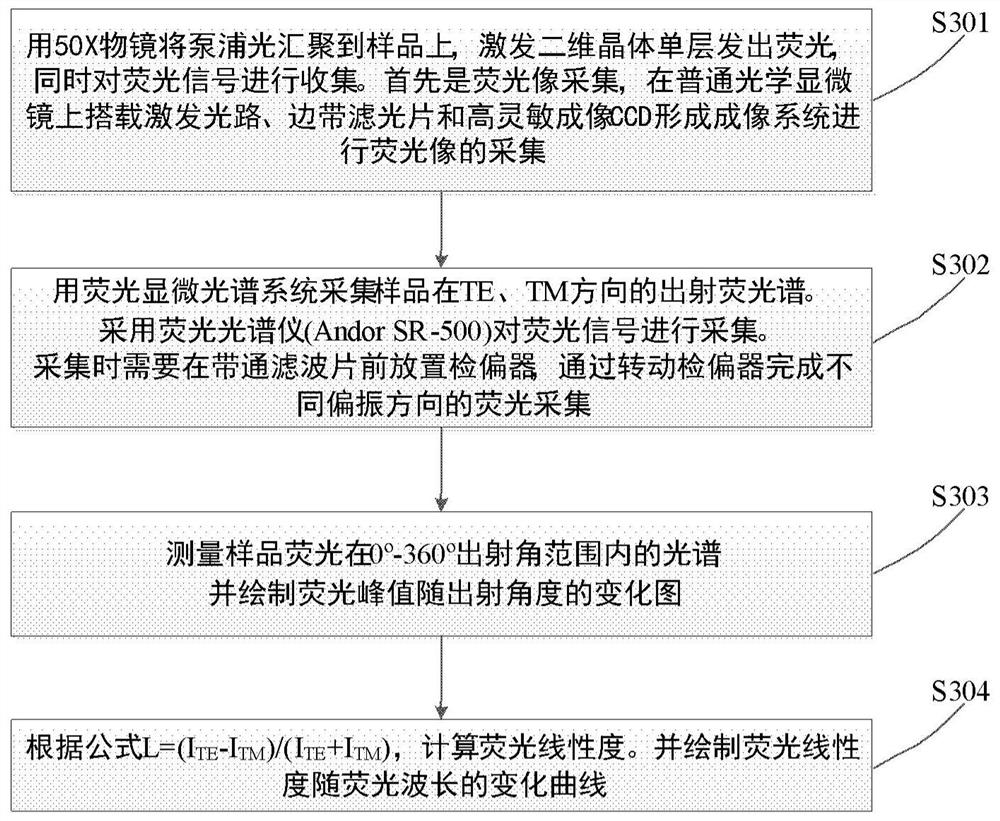
[0103] Figure 4A is the WS 2 Optical microscopy imaging of monolayers. Figure 4B is the emission fluorescence spectrum in the TE and TM directions obtained through the test in step S302. Depend on Figure 4B It can be seen that the fluorescence intensity of the sample is equal in the TE and TM directions, and the WS 2 The fluorescence peak of the monolayer is at ~630nm, the full width at half maximum is ~30nm, and the forbidden band width is 1.9-2.0eV. Figure 4C It is a diagram of the variation of the fluorescence spectrum with the exit angle obtained through the test in step S303. Depend on Figure 4C It can be seen th...
Embodiment 2
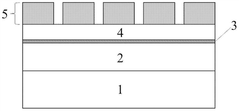
[0104] Example 2: Ag nanowire grid pair WS 2 Device for Modulating the Polarization of Forbidden Fluorescence
[0105] Since the modulation method proposed in the present invention is based on the principle of metamaterial surface plasmon resonance, which is affected by the shape of the metamaterial, three metal nano-metamaterials with three shapes are designed to modulate the fluorescence linearity in this example. They are nano wire grid, V type nano grid and N type nano grid.
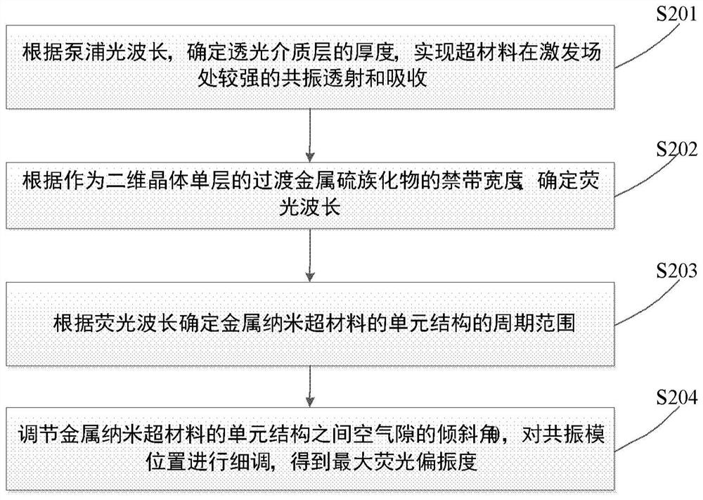
[0106] The period selection of the unit structure is determined according to the fluorescence wavelength of the two-dimensional crystal. For example, the periods of N and V-type nanostructures in the TE and TM polarization directions can be set to 200nm and 400nm respectively, so that the metamaterial surface plasmon resonance will be in the monolayer WS 2 Fluorescence wavelength ~ 630nm generated near. Further adjustment of the inclination angle of the air gap in the structural unit can adjust th...
Embodiment 3
[0129] In addition to the above systems, the preferred two-dimensional crystals are single-layer WSe 2 . WS 2 The monolayer has higher quantum efficiency and longer fluorescence wavelength 750nm. by the WSe 2 The structure and process of the single-layer preparation metamaterial-two-dimensional crystal bandgap fluorescence polarization modulation device are the same as in Example 2. The period of the selected nanostructure should be determined according to the fluorescence wavelength, and the thickness of the selected medium layer is determined by the wavelength of the excitation light. The principles are described in the Technical Program Brief. Generally, the wavelength increases, the metal dissipation decreases, the surface plasmon resonance response increases, and the effect on fluorescence linearity modulation is better.
PUM
| Property | Measurement | Unit |
|---|---|---|
| Thickness | aaaaa | aaaaa |
| Thickness | aaaaa | aaaaa |
| Thickness | aaaaa | aaaaa |
Abstract
Description
Claims
Application Information
 - R&D
- Intellectual Property
- Life Sciences
- Materials
- Tech Scout
- Unparalleled Data Quality
- Higher Quality Content
- 60% Fewer Hallucinations
Browse by: Latest US Patents, China's latest patents, Technical Efficacy Thesaurus, Application Domain, Technology Topic, Popular Technical Reports.
© 2025 PatSnap. All rights reserved.Legal|Privacy policy|Modern Slavery Act Transparency Statement|Sitemap|About US| Contact US: help@patsnap.com


