
Manufacturing process of SMD1612 crystal resonator

A technology of SMD1612 and crystal resonator, applied in the direction of electrical components, impedance network, etc., can solve the problems of complex packaging process, high equipment investment cost, complex phase diagram of gold-tin binary alloy, etc., to reduce costs, avoid product loss, Reliable and stable sealing effect

Inactive Publication Date: 2020-09-25
江苏浩都频率科技有限公司
View PDF0 Cites 0 Cited by
  • Summary
  • Abstract
  • Description
  • Claims
  • Application Information

AI Technical Summary

Problems solved by technology

Most domestic factories are still in the research and development stage, and their main process technology is still in the hands of foreign factories such as Japan. The manufacturing process of SMD1612 crystal resonators in Japan is mainly based on gold-tin (AUSN) soldering, and the packaging process is complicated. Based on the eutectic composition of the alloy, the melting point of gold-tin eutectic solder is 280°C, and the soldering temperature is 300°C-310°C, so that the alloy melts and wets the device to achieve soldering, but the phase diagram of the gold-tin binary alloy is very complicated, and there are many Intermediate phases, these intermediate phases are hard and brittle phases, alloys of all components of gold-tin are composed of these gold-tin intermediate phases
Therefore, the material and equipment input costs of this gold-tin soldering process are high, and the materials and equipment are all dependent on imports from Japan, and the main materials in Japan are restricted from exporting to China due to technical protection. Therefore, domestic purchases can only be made from Japan at high prices. Ultra Miniaturized Crystal Units

Method used


Image

  • Manufacturing process of SMD1612 crystal resonator
  • Manufacturing process of SMD1612 crystal resonator
  • Manufacturing process of SMD1612 crystal resonator

Examples


Embodiment Construction

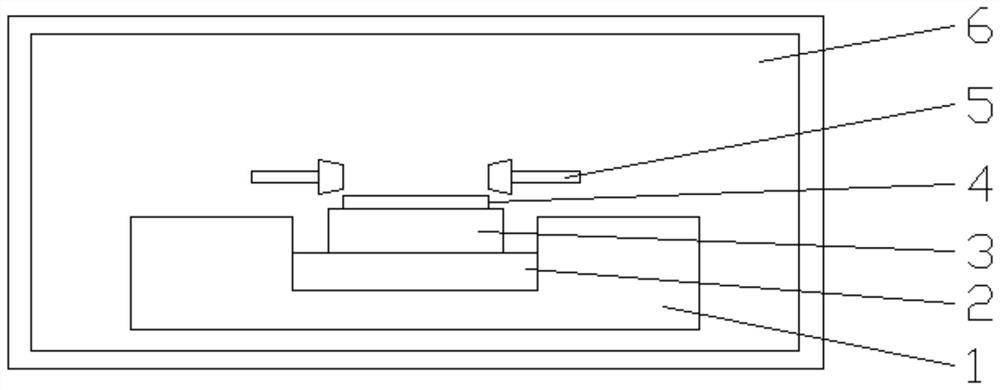
[0024] The present invention is described in further detail now in conjunction with accompanying drawing. These drawings are all simplified schematic diagrams, which only illustrate the basic structure of the present invention in a schematic manner, so they only show the configurations related to the present invention.

[0025] Such as figure 1 Shown, a kind of manufacturing process of SMD1612 crystal resonator comprises the following steps:

[0026] Pre-washing→arraying→post-washing→coating→glue dispensing→curing→fine-tuning→seal welding→aging→reflow solderingleak detection→test printing taping→packaging→storage;

[0027] In the wafer arrangement step: the length of the wafer is 1.04-1.1mm, and the width of the wafer is 0.64-0.85mm;

[0028] In the glue dispensing step: use the cut-in method to load the chip, the chip loading position is controlled at 1 / 2 to 1 / 3 of the primer, and the chip angle when loading and cutting is 1-3 degrees;

[0029] In the fine-tuning step: th...


PUM


Abstract

The invention discloses a manufacturing process of an SMD1612 crystal resonator. The manufacturing process comprises the following steps of pre-washing, wafer arrangement, post-washing, film coating,dispensing, curing, fine adjustment, seal welding, aging, reflow welding, leakage detection, test printing braid, packaging and warehousing. A wafer is carried in a cut-in mode, the carrying positionof the wafer is controlled to be 1 / 2-1 / 3 of the position of a primer, the angle of the wafer is controlled to be 1-3 degrees during carrying and cutting-in, the risk that the tail of the wafer warps upwards is controlled, it is guaranteed that the primer can wrap the wafer, and various reliability performance tests such as thrust and falling are met; a hot melting diffusion bonding technology is adopted, an upper layer plate, a lower layer plate and a fine adjustment plate pore plate are subjected to diffusion bonding to form an integrated fine adjustment plate, the stability of electrical characteristics of a product is improved, meanwhile, product loss caused by manual assembly errors is avoided, and the production efficiency is improved; a parallel welding process is adopted for packaging and welding, a gold soldering process is replaced, and the reliable and stable sealing and welding effect can be achieved while the cost is reduced.

Description

technical field [0001] The invention relates to the technical field of power electronics, in particular to a manufacturing process of an SMD1612 crystal resonator. Background technique [0002] With the development trend of multi-function and miniaturization of electronic products, crystal resonators are key electronic components, and the market demand for high-precision and miniaturized products is increasing. The development of SMD surface mount crystal resonators is also from 7050→6035→ 5032→3225→2520→2016 The trend of getting smaller and smaller is gradually developing. [0003] At present, the market has mature technology for the products of the above specifications, because the smaller the product, the more difficult it is to achieve high performance, and the higher the requirements for technology and precision. Most domestic factories are still in the research and development stage, and their main process technology is still in the hands of foreign factories such as ...

Claims


Application Information

Patent Timeline
Patent Type & Authority Applications(China)
IPC IPC(8): H03H3/04
CPCH03H3/04H03H2003/0414H03H2003/0457
Inventor 王秋贞吴佳斌
Owner 江苏浩都频率科技有限公司
Learn More