
Photosensitive detector based on transverse depletion of composite dielectric gate and method thereof

A photosensitive detector and composite medium technology, applied in the direction of electric solid state devices, semiconductor devices, electrical components, etc., can solve the problem that the safety and reliability are difficult to guarantee, cannot generate enough deep depletion region, and the response wavelength range is limited, etc. problem, to achieve the effect of wide dynamic range, low noise and high quantum efficiency

Active Publication Date: 2020-08-14
NANJING UNIV
View PDF5 Cites 2 Cited by
  • Summary
  • Abstract
  • Description
  • Claims
  • Application Information

AI Technical Summary

Problems solved by technology

However, in order to obtain a larger and deeper depletion region to obtain a higher and wider-band photoresponse, the dual-transistor photosensitive detector needs to apply a large positive bias voltage on the gate substrate, which is not conducive to the realization of the system, its safety and Reliability is also difficult to guarantee
Especially after the isolation implant is added to the P-type photosensitive area, since the isolation is P+-type ion implantation, the isolation will be exhausted during the working process, resulting in the inability to generate a depletion region with sufficient depth, and the range of response wavelengths is severely restricted.

Method used


Image

  • Photosensitive detector based on transverse depletion of composite dielectric gate and method thereof
  • Photosensitive detector based on transverse depletion of composite dielectric gate and method thereof
  • Photosensitive detector based on transverse depletion of composite dielectric gate and method thereof

Examples


Embodiment Construction

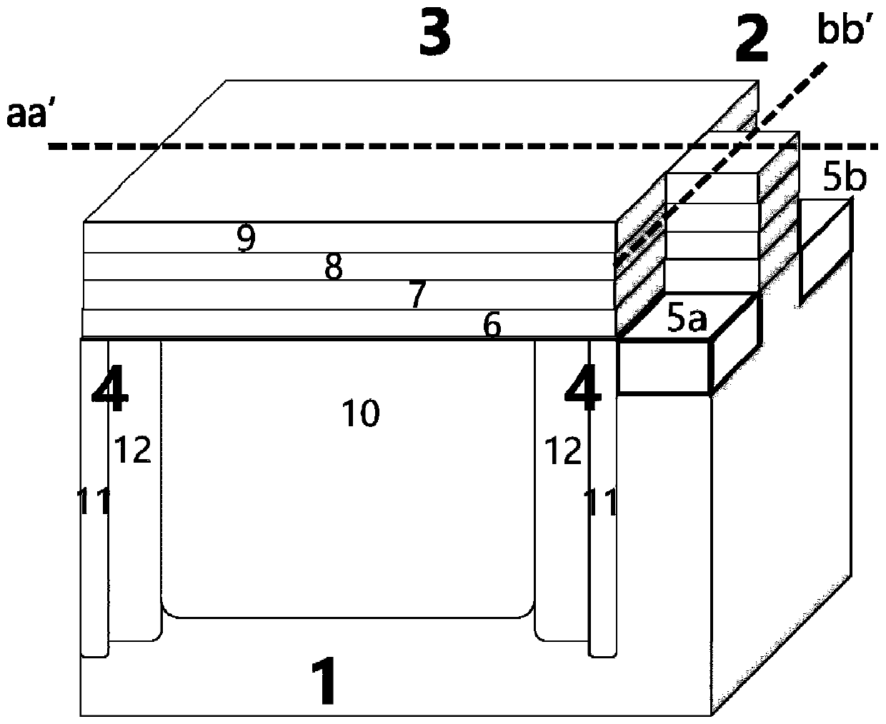
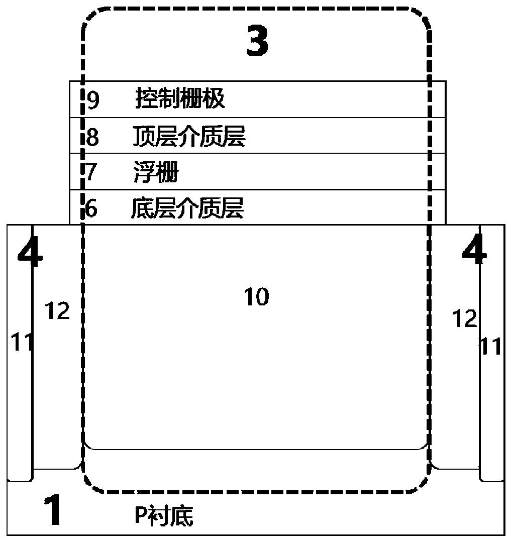
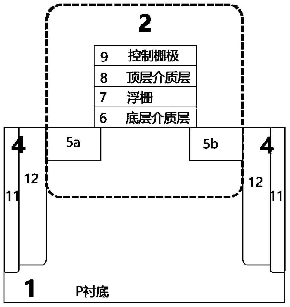
[0030] This embodiment provides a device structure based on a composite dielectric gate laterally depleted photosensitive detector. The detector unit is fabricated on the same P-type substrate, including a composite dielectric gate transistor 2 with a reading function and a composite dielectric with a photosensitive function. The gate MOS capacitor 3 is provided with a P / P+ doped region with an isolation function in the substrate between the two.

[0031] like Figure 1-4 As shown, the transistor 2 and the MOS capacitor 3 of the detector unit share a composite dielectric gate, which includes a bottom insulating dielectric layer 6 , a floating gate 7 , a top dielectric layer 8 and a control gate 9 from top to bottom. image 3 Among them, for the composite dielectric gate transistor 2, there are N-type source 5a and drain 5b formed by ion implantation on the surface of the substrate, which can be regarded as an ordinary floating gate transistor alone. figure 1 and 2 Among them...


PUM


Abstract

The invention discloses a photosensitive detector based on the transverse depletion of a composite dielectric gate and a method thereof. A unit of the detector comprises a composite dielectric gate MOS capacitor and a composite dielectric gate transistor which are formed above the same P-type semiconductor substrate, wherein the composite dielectric gate transistor comprises a source-drain region,a first bottom insulating dielectric layer, a first floating gate, a first top insulating dielectric layer and a first control gate; the composite dielectric gate MOS capacitor is sequentially provided with a second bottom insulating dielectric layer, a second floating gate, a second top insulating dielectric layer and a second control gate on the substrate, and the first floating gate is connected with the second floating gate; an N or N-type photosensitive region is arranged in a substrate of the composite dielectric gate MOS capacitor; and a P or P+ type isolation region is arranged aroundthe photosensitive region and is used for separating the composite dielectric gate transistor from the composite dielectric gate MOS capacitor. The quantum efficiency of the detector can be improved,the wavelength range of light response is expanded, and the noise caused by recombination generated by the surface energy level is reduced.

Description

technical field [0001] The invention relates to an imaging detection device, especially the structure and working mechanism of an imaging detection device in the infrared, visible light band to ultraviolet band, and in particular to a photosensitive detector based on composite dielectric grid lateral depletion and a method thereof. Background technique [0002] CCD and CMOS-APS are the two most common imaging devices at present. The basic structure of the CCD that appeared earlier is a group of MOS capacitors connected in series. The generation and change of the potential well on the semiconductor surface is controlled by the pulse timing on the MOS capacitor, so as to realize the storage and transfer of photogenerated charges. This kind of method causes the imaging speed of CCD to be slower, and CCD is extremely high to the requirement of technology simultaneously, makes its yield rate low, and cost is bigger. CMOS-APS usually consists of a photosensitive diode and three t...

Claims


Application Information

Patent Timeline
Patent Type & Authority Applications(China)
IPC IPC(8): H01L27/146H01L29/423
CPCH01L27/14614H01L29/42364H01L29/42324H01L27/1463Y02P70/50
Inventor 闫锋沈凡翔李张南王子豪王凯顾郅扬胡心怡柴智
Owner NANJING UNIV
Learn More