Composite silicon substrate, preparation method and application thereof

A silicon substrate and silicon layer technology, applied in chemical instruments and methods, from chemical reactive gases, semiconductor/solid-state device manufacturing, etc., can solve the problems of increasing epitaxial thickness, high substrate price, substrate supply stability, and increasing final Problems such as device cost can be achieved by increasing the working voltage of the device, making the preparation method simple, and improving the quality of the crystal.

Active Publication Date: 2020-07-31
HUNAN SANAN SEMICON CO LTD
View PDF12 Cites 0 Cited by
  • Summary
  • Abstract
  • Description
  • Claims
  • Application Information

AI Technical Summary

Problems solved by technology

Both of the above two methods have certain defects. The use of a thicker substrate will cause the epitaxial wafer to be incompatible with the chip manufacturing equipment and increase the thickness of the epitaxial layer. Higher price and issues with substrate supply stability, thus increasing final device cost

Method used


Image

  • Composite silicon substrate, preparation method and application thereof
  • Composite silicon substrate, preparation method and application thereof
  • Composite silicon substrate, preparation method and application thereof

Examples


Embodiment 1

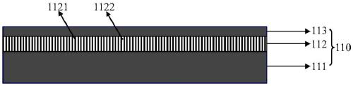
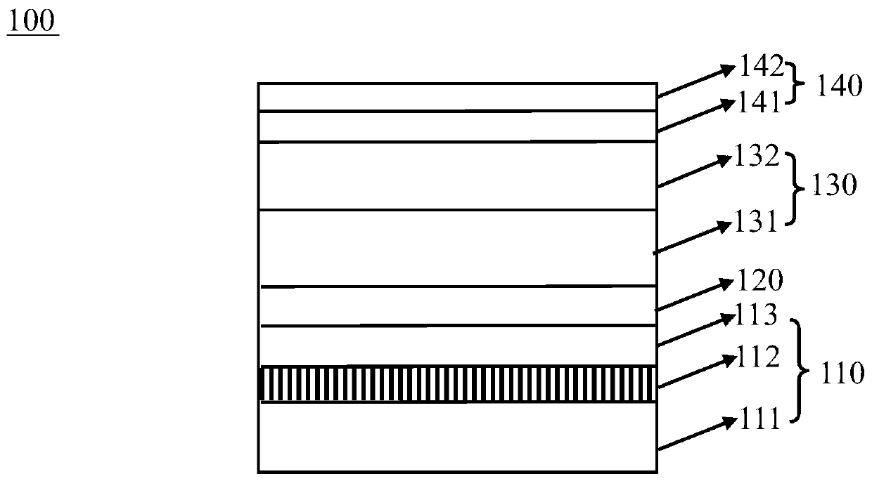
[0025] refer to figure 1 , a composite silicon substrate 110 includes a first silicon layer 111, a patterned silicon layer 112 and a second silicon layer 113, and the patterned silicon layer 112 is sandwiched between the first silicon layer 111 and the second silicon layer 113 An array of submicron pillars 1121 , the spacing of the submicron pillars forms a cavity 1122 .

[0026] The making of composite silicon substrate 110: throw a layer of about 1um thick photoresist AZ2460 on the front side of the silicon substrate of the (111) crystal plane, and then use the method of laser interference exposure to make a period (that is, adjacent sub-substrates) on the photoresist. Micron column interval) 500nm, photoresist point array pattern with a diameter of 200nm; then use the ICP etching method to transfer the submicron pattern of the photoresist to the silicon substrate; etch the depth on the silicon substrate by ICP The patterned silicon layer 112 of the array of 8um silicon sub...

Embodiment 2

[0029] The difference between embodiment 2 and embodiment 1 is that the second silicon layer is formed by bonding a thin silicon layer with a thickness of about 10 um (111) on the patterned silicon layer by using the Smart-cut method.

Embodiment 3

[0031] The difference between embodiment 3 and embodiment 1 is that the patterned silicon layer is porous silicon interposed between the first silicon layer and the second silicon layer, and the pores of the porous silicon form cavities.

[0032] Production method: Put the low-resistance silicon substrate as the anode into the mixed solution of hydrofluoric acid, deionized water and absolute ethanol, and metal platinum (Pt) as the cathode, and conduct electrochemical corrosion on the silicon substrate with an appropriate current A layer of porous silicon structure is formed on the surface of the substrate. By controlling the electrochemical corrosion conditions and the resistivity of the substrate, a porous silicon layer with a pore size of 100nm-1um can be prepared. The thickness of the porous silicon layer is about 10um, and the porosity (that is, the pores occupy The volume of the porous silicon layer) is between 20%-80%, more preferably 40%-60%, so as to ensure that the obt...


PUM

PropertyMeasurementUnit
pore sizeaaaaaaaaaa
sizeaaaaaaaaaa
thicknessaaaaaaaaaa

Abstract

The invention discloses a composite silicon substrate and a preparation method thereof. The composite silicon substrate comprises a first silicon layer, a graphical silicon layer and a second siliconlayer, wherein the second silicon layer forms a surface for heteroepitaxial growth, and the graphical silicon layer is clamped between the first silicon layer and the second silicon layer and forms aplurality of micro-nano cavities to attenuate stress transmitted from the second silicon layer to the first silicon layer. According to the composite silicon substrate, the storage pressure stress inheteroepitaxial growth can be increased, the warping of the substrate can be reduced, and a thick heteroepitaxial film can be grown. The invention further discloses a gallium nitride epitaxial structure based on the composite silicon substrate, wherein vertical electric leakage of the buffer layer is effectively reduced, the electrical property of the device is improved, possibility is provided for manufacturing of a silicon-based gallium nitride high-voltage device, and the gallium nitride epitaxial structure is suitable for actual production and application.

Description

technical field [0001] The invention relates to the technical field of semiconductor devices, in particular to a composite silicon substrate and its preparation method and application. Background technique [0002] At present, due to the lack of high-quality, large-scale commercial gallium nitride substrates, gallium nitride-based device thin film materials are generally grown on sapphire, silicon carbide, silicon and other substrates by heteroepitaxy. As an important gallium nitride heteroepitaxy substrate, silicon substrate has high crystal quality, large wafer size, high thermal conductivity (about 3 times that of sapphire), low price, and substrate conductivity can be improved by doping Control and other advantages, and thus more and more attention by the industry. When heteroepitaxially growing GaN thin films on silicon substrates, there are two main technical difficulties: one is that there is a large lattice mismatch (16.9%) between the GaN epitaxial film and the sil...

Claims


Application Information

Patent Timeline
Patent Type & Authority Applications(China)
IPC IPC(8): H01L21/02H01L29/778H01L33/12C30B25/04C30B29/40
CPCH01L29/7786H01L33/12H01L21/02381H01L21/02428H01L21/02458H01L21/0254H01L21/0262C30B29/406C30B25/04
Inventor 蔡文必房育涛刘波亭李健张恺玄
Owner HUNAN SANAN SEMICON CO LTD
Why Eureka
Try Eureka