


Quick Research
Generate reliable direction feasibility study reports for your R&D in just a few steps.

Technical Q&A
Discover and master advanced knowledge NOW. Basics, ideas, possibilities, all at once.

Find Solutions
As an expert in R&D theories, this can generate solutions to your technical problems instantly.

Evaluate Feasibility
Analyze your overall solution with one click, know your potential R&D risks in advance.

Monitor Landscape
Get weekly tech updates, stay abreast of the latest tech innovations and key insights.
Micro-cavity structure top emitting device and preparation method thereof
A top emission and microcavity technology, applied in the field of microcavity structure top emission devices and their preparation, can solve the problems of restricting the application of inkjet printing technology, high material requirements, and high production costs, and achieves easy control of film thickness, simple equipment, and high production cost. low cost effect
- Summary
- Abstract
- Description
- Claims
- Application Information
AI Technical Summary
Problems solved by technology
Method used
Image

Examples
preparation example Construction
[0028] The invention provides a method for preparing a top-emitting device with a microcavity structure, comprising the following steps:
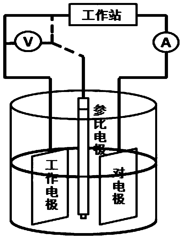
[0029] Using the anode substrate as a working electrode, performing a first electrochemical polymerization in a first electrolyte solution to obtain an anode substrate deposited with a hole transport layer; the first electrolyte solution contains a hole transport electroactive monomer and a supporting electrolyte;
[0030] The anode substrate deposited with the hole transport layer is used as a working electrode, and the second electrochemical polymerization is carried out in the second electrolyte to form a white light-emitting layer on the surface of the hole transport layer; the second electrolyte contains white hair Photoactive monomers and supporting electrolytes;
[0031] An electron transport layer, an electron injection layer and a cathode layer are sequentially vapor-deposited on the surface of the white luminescent layer to obtain...
Embodiment 1
[0071] 1) Preparation of the anode layer of the top emission device
[0072] Sputtering ITO with a thickness of 90nm on metal Al with a thickness of 150nm to obtain an anode substrate;
[0073] 2) Preparation of hole transport layer
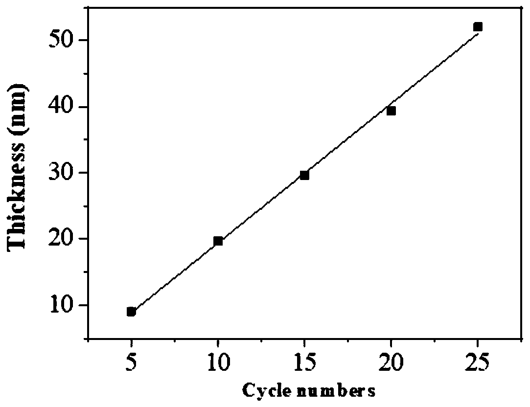
[0074] The anode substrate Al / ITO is used as a working electrode, the electroactive precursor molecule in the electrolyte used is 4,4',4"-tris(carbazol-9-yl)triphenylamine (TCTA), and the supporting electrolyte is four Butyl ammonium hexafluorophosphate (TBAPF 6 ), the solvent of the electrolyte is a mixed solvent of dichloromethane, acetonitrile and propylene carbonate (volume ratio is 2.5:0.9:1.6), and the concentration of TCTA in the electrolyte is 4×10 -4 mol / L, the concentration of the supporting electrolyte in the electrolyte is 0.1mol / L; the first electrochemical polymerization is carried out in the above electrolyte by cyclic voltammetry, the scanning voltage range is -0.6 ~ 1.22V, and the scanning speed is 300mV / S, the number of scan...
Embodiment 2
[0086] The preparation process of the top-emitting device of this embodiment is the same as that of Embodiment 1, the only difference is:
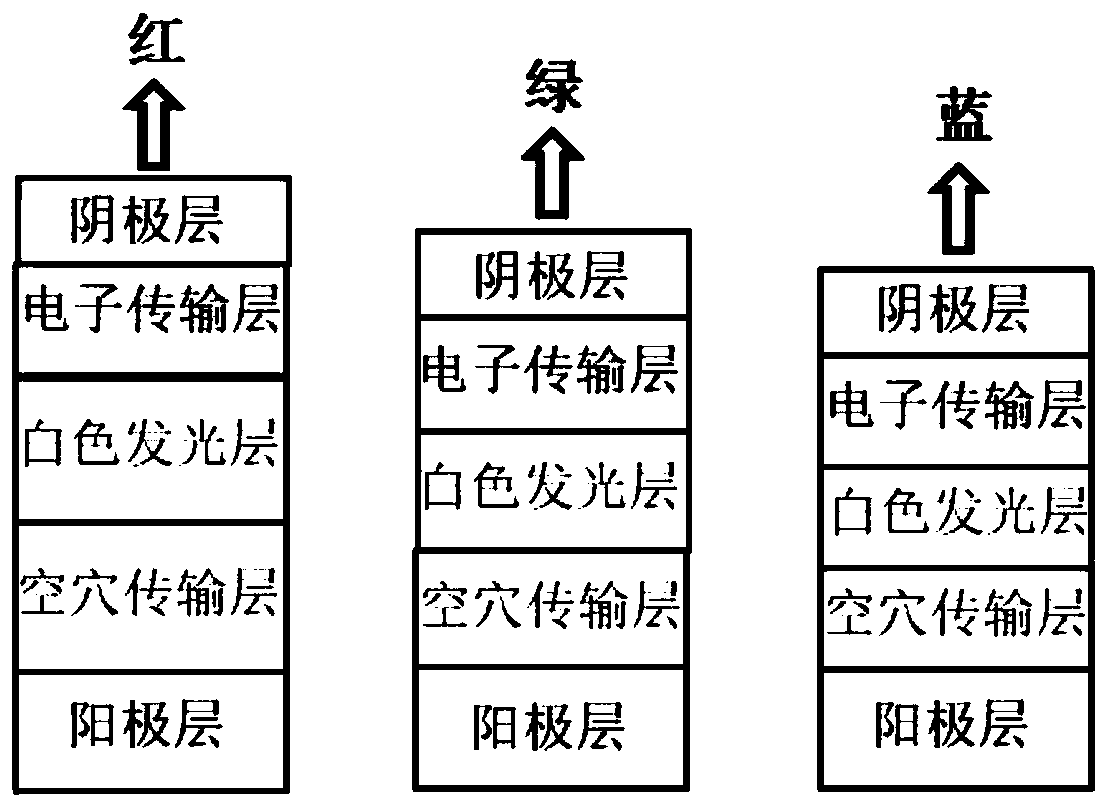
[0087] Design the anode substrate (referring to the metal reflective layer and ITO layer) of the top-emitting device as a red, green and blue array layout, such as Figure 4Shown: the pixels in each column of the substrate are connected together, and there is no conduction between the columns. When the electricity is turned on, the conductive state of the pixels in the columns is consistent, and whether the pixels in each column are powered is determined by the external circuit. Since the electropolymerization process only occurs in the energized area, the electroactive precursor molecules will not undergo redox reactions and then be deposited on the substrate in the non-energized area. Therefore, different thicknesses can be deposited by controlling the on-off state of each column of pixels. film. For example, when the first and fourth c...
PUM
| Property | Measurement | Unit |
|---|---|---|
| thickness | aaaaa | aaaaa |
| thickness | aaaaa | aaaaa |
| thickness | aaaaa | aaaaa |
Abstract
Description
Claims
Application Information
 - R&D Engineer
- R&D Manager
- IP Professional
- Industry Leading Data Capabilities
- Powerful AI technology
- Patent DNA Extraction
Browse by: Latest US Patents, China's latest patents, Technical Efficacy Thesaurus, Application Domain, Technology Topic, Popular Technical Reports.
© 2024 PatSnap. All rights reserved.Legal|Privacy policy|Modern Slavery Act Transparency Statement|Sitemap|About US| Contact US: help@patsnap.com