


Quick Research
Generate reliable direction feasibility study reports for your R&D in just a few steps.

Technical Q&A
Discover and master advanced knowledge NOW. Basics, ideas, possibilities, all at once.

Find Solutions
As an expert in R&D theories, this can generate solutions to your technical problems instantly.

Evaluate Feasibility
Analyze your overall solution with one click, know your potential R&D risks in advance.

Monitor Landscape
Get weekly tech updates, stay abreast of the latest tech innovations and key insights.
Self-powered perovskite photoelectric detector and preparation method thereof
A photodetector, perovskite technology, applied in photovoltaic power generation, electric solid-state devices, semiconductor/solid-state device manufacturing, etc. It can reduce the non-radiative recombination rate and dark current density, facilitate efficient transmission, reduce the cost of devices and the complexity of the production process.
- Summary
- Abstract
- Description
- Claims
- Application Information
AI Technical Summary
Problems solved by technology
Method used
Image

Examples
preparation example Construction
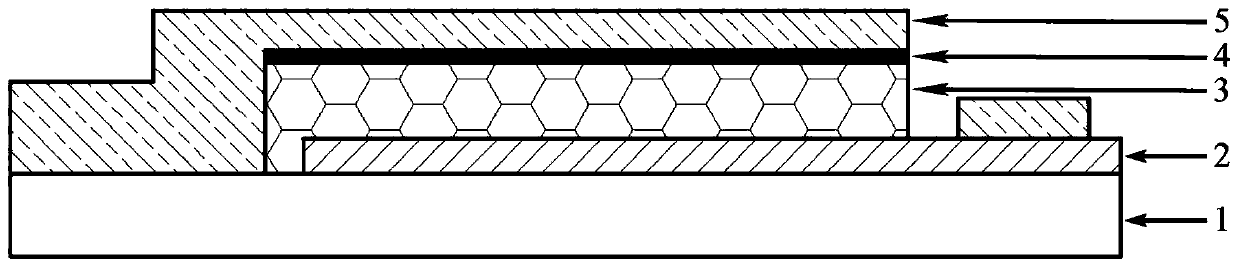
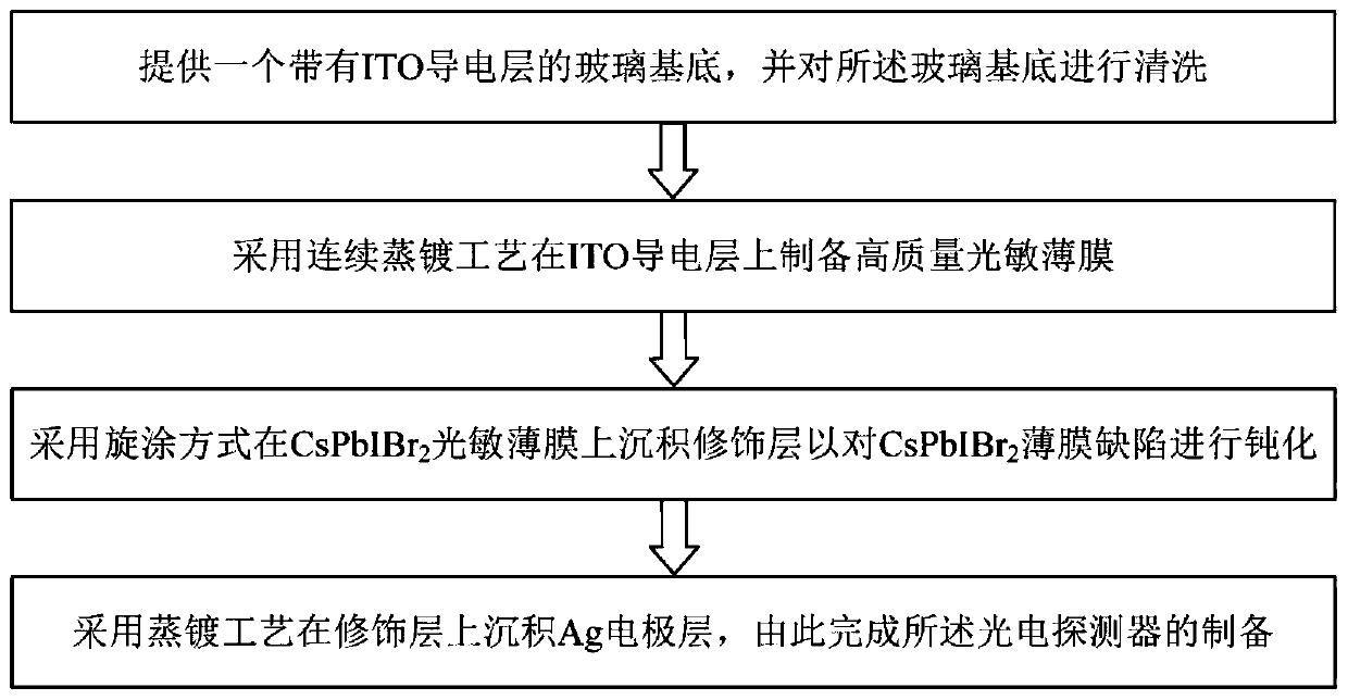
[0034] see figure 2 and image 3 , the present invention also provides a kind of preparation method of self-powered perovskite photodetector, described preparation method comprises the following steps:
[0035] Step 1, providing a glass substrate with an ITO conductive layer, and cleaning the glass substrate.
[0036] Specifically, a glass substrate with an ITO conductive layer is provided, and the glass substrate is ultrasonically cleaned for 10 minutes to 20 minutes using cleaning agent, acetone, ethanol and deionized water in sequence; then, the glass substrate is cleaned with N 2 After the airflow dries the glass substrate, the glass substrate is treated with ultraviolet and ozone for 20 minutes to 30 minutes.
[0037] Step 2, preparing a high-quality photosensitive film on the ITO layer by using a continuous evaporation process.
[0038] Specifically, a photosensitive film is prepared by a continuous evaporation process on the glass substrate with an ITO conductive la...
Embodiment 1
[0046] The preparation method of a self-powered perovskite photodetector provided by the first embodiment of the present invention mainly includes the following steps:
[0047] S1, providing a glass substrate with an ITO conductive layer, and cleaning the glass substrate.
[0048] Specifically, a glass substrate with an ITO conductive layer is provided, and the glass substrate is ultrasonically cleaned for 15 min with cleaning agent, acetone, ethanol and deionized water in sequence, and then cleaned with N 2 Airflow blows dry described glass substrate, then carries out ultraviolet ozone treatment 25min to described glass substrate;
[0049] S2, using a continuous evaporation process to prepare a high-quality photosensitive film on the ITO conductive layer.
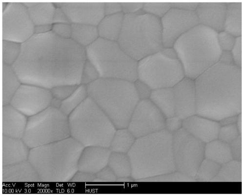
[0050] Specifically, a photosensitive film is prepared by a continuous evaporation process on the ITO conductive layer, and the photosensitive film is an inorganic CsPbIBr 2 Photosensitive thin film, which is obtained by...
Embodiment 2
[0057] The preparation method of a self-powered perovskite photodetector without a charge transport layer provided by the second embodiment of the present invention mainly includes the following steps:
[0058] B1, providing a glass substrate with an ITO conductive layer, and cleaning the glass substrate.
[0059] Specifically, a glass substrate with an ITO conductive layer was provided, and the glass substrate was ultrasonically cleaned for 20 min with cleaning agent, acetone, ethanol and deionized water in sequence, and then cleaned with N 2 Dry the glass substrate by air flow, and then carry out ultraviolet and ozone treatment on the glass substrate for 30min;
[0060] B2, using a continuous evaporation process to prepare a high-quality photosensitive film on the ITO conductive layer.
[0061] Specifically, a photosensitive film is prepared on a glass substrate with an ITO conductive layer by a continuous evaporation process, and the photosensitive film is an inorganic CsP...
PUM
| Property | Measurement | Unit |
|---|---|---|
| Thickness | aaaaa | aaaaa |
| Thickness | aaaaa | aaaaa |
| Thickness | aaaaa | aaaaa |
Abstract
Description
Claims
Application Information
 - R&D Engineer
- R&D Manager
- IP Professional
- Industry Leading Data Capabilities
- Powerful AI technology
- Patent DNA Extraction
Browse by: Latest US Patents, China's latest patents, Technical Efficacy Thesaurus, Application Domain, Technology Topic, Popular Technical Reports.
© 2024 PatSnap. All rights reserved.Legal|Privacy policy|Modern Slavery Act Transparency Statement|Sitemap|About US| Contact US: help@patsnap.com