


Quick Research
Generate reliable direction feasibility study reports for your R&D in just a few steps.

Technical Q&A
Discover and master advanced knowledge NOW. Basics, ideas, possibilities, all at once.

Find Solutions
As an expert in R&D theories, this can generate solutions to your technical problems instantly.

Evaluate Feasibility
Analyze your overall solution with one click, know your potential R&D risks in advance.

Monitor Landscape
Get weekly tech updates, stay abreast of the latest tech innovations and key insights.
P-type nitrogen-doped gallium oxide film and preparation method thereof
A technology for thin film preparation and nitrogen doping, which can be used in final product manufacturing, sustainable manufacturing/processing, semiconductor/solid-state device manufacturing, etc. , the effect of high repetition rate and high doping rate
- Summary
- Abstract
- Description
- Claims
- Application Information
AI Technical Summary
Problems solved by technology
Method used
Image


Examples
Embodiment 1
[0065] Embodiment 1: This embodiment provides a p-type gallium oxide thin film and its growth method
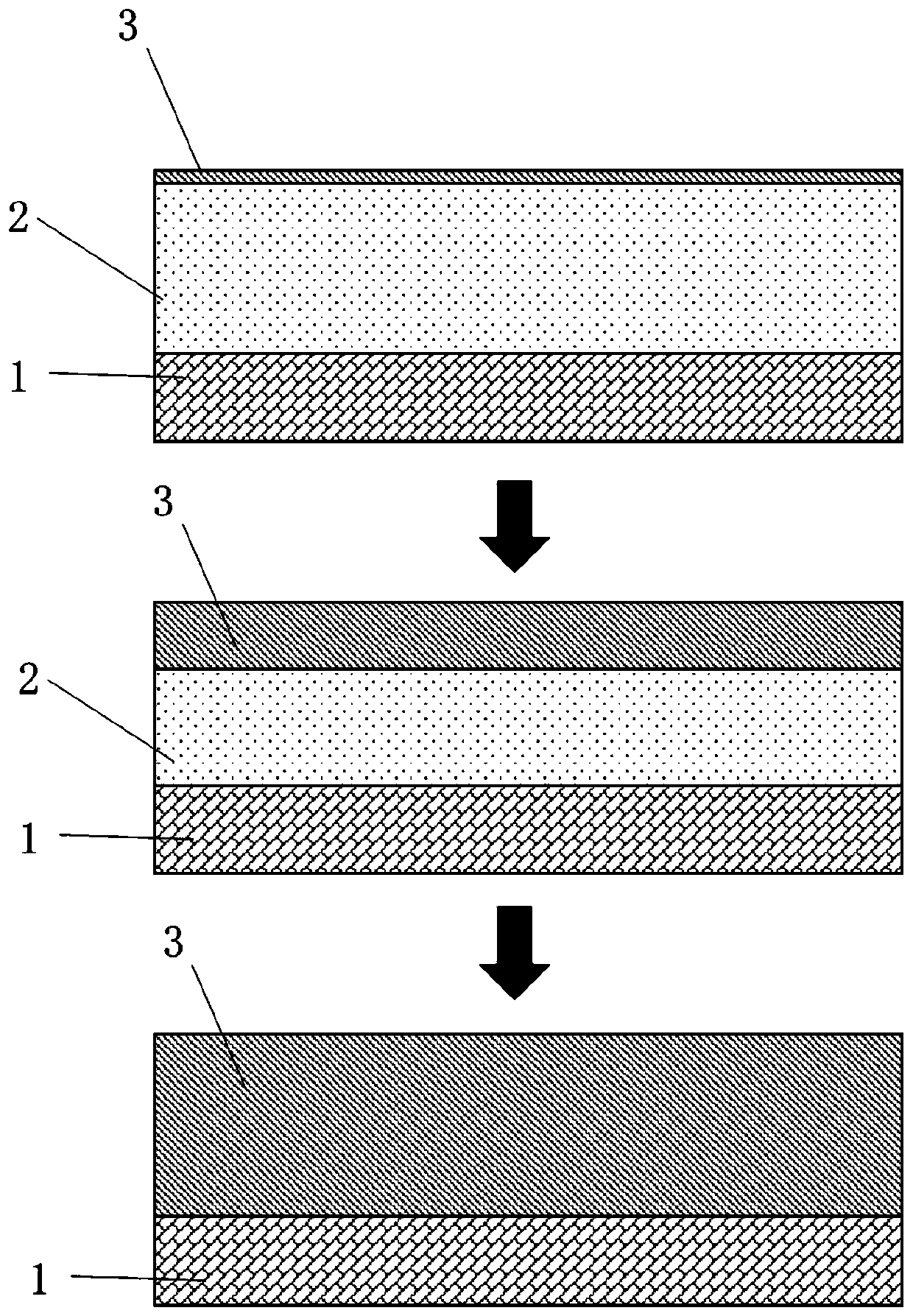
[0066] Such as figure 2 Shown, for preparing P-type nitrogen-doped gallium oxide film preparation method, comprises the following steps:
[0067] (1) Place a gallium nitride film in the cavity to form a specific oxygen content in the cavity
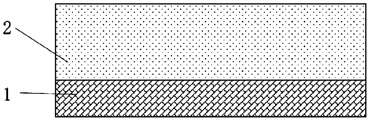
[0068] Such as figure 1 Shown is a schematic diagram of a gallium nitride film. After the gallium nitride film including the substrate is placed in the chamber of the chemical vapor deposition equipment, the pressure in the chamber of the chemical vapor deposition equipment is kept stable at 1.01×10 3 Pa, and continuously feed argon with a flow rate of 700 sccm for 120 minutes, so that the cavity reaches 1.0×10 -15 the hypoxic environment.
[0069] (2) High temperature growth of gallium oxide thin film
[0070] up to 1.0×10 -15 After the low-oxygen environment, the argon flow rate was reduced to 200 sccm, and the chamber pressure ...
Embodiment 2
[0078] Embodiment 2: This embodiment provides a preparation method of a top-gate transistor based on p-type gallium oxide
[0079] Such as Figure 8 Shown is a schematic diagram of a transistor, the transistor structure includes a p-type nitrogen-doped gallium oxide thin film structure, source electrodes and drain electrodes located at both ends of the gallium oxide thin film structure, a first insulating layer located in the center of the gallium oxide thin film structure, A gate electrode on the first insulating layer, a second insulating layer on the source electrode, the drain electrode, the gate electrode and the p-type nitrogen-doped gallium oxide structure.
[0080] The preparation method of the top-gate transistor comprises the following steps:
[0081] (1) Place a gallium nitride film in the cavity to form a specific oxygen content in the cavity
[0082] After putting the gallium nitride film containing the substrate into the chamber of the chemical vapor deposition...
example 2
[0094] The Schottky contact existing in the device in Example 2 can be improved into an ohmic contact by improving the metal-semiconductor contact through electrode material selection, material interface treatment before electrode deposition, etc.
PUM
| Property | Measurement | Unit |
|---|---|---|
| Surface roughness | aaaaa | aaaaa |
| Resistivity | aaaaa | aaaaa |
| Thickness | aaaaa | aaaaa |
Abstract
Description
Claims
Application Information
 - R&D Engineer
- R&D Manager
- IP Professional
- Industry Leading Data Capabilities
- Powerful AI technology
- Patent DNA Extraction
Browse by: Latest US Patents, China's latest patents, Technical Efficacy Thesaurus, Application Domain, Technology Topic, Popular Technical Reports.
© 2024 PatSnap. All rights reserved.Legal|Privacy policy|Modern Slavery Act Transparency Statement|Sitemap|About US| Contact US: help@patsnap.com