


Quick Research
Generate reliable direction feasibility study reports for your R&D in just a few steps.

Technical Q&A
Discover and master advanced knowledge NOW. Basics, ideas, possibilities, all at once.

Find Solutions
As an expert in R&D theories, this can generate solutions to your technical problems instantly.

Evaluate Feasibility
Analyze your overall solution with one click, know your potential R&D risks in advance.

Monitor Landscape
Get weekly tech updates, stay abreast of the latest tech innovations and key insights.
Super junction structure and manufacturing method thereof
A technology of superjunction and unit structure, applied in the fields of semiconductor/solid-state device manufacturing, semiconductor devices, electrical components, etc., can solve problems such as affecting device consistency, device performance deviation, and increasing the difficulty of process control.
- Summary
- Abstract
- Description
- Claims
- Application Information
AI Technical Summary
Problems solved by technology
Method used
Image

Examples
no. 1 example
[0075] The super junction structure of the first embodiment of the present invention:
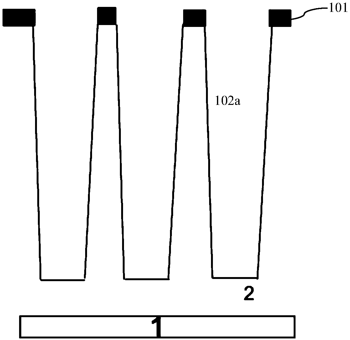
[0076] Such as Figure 1C Shown is the device structure diagram of the super junction structure of the first embodiment of the present invention; figure 2 It is a device structure diagram of a super-junction device formed by adopting the super-junction structure of the first embodiment of the present invention. The super-junction structure of the first embodiment of the present invention includes:
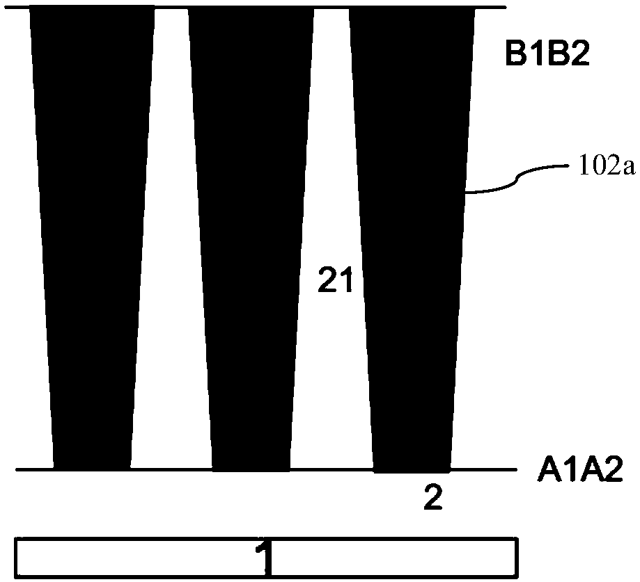
[0077] The first N-type sub-epitaxial layer 2 is formed in the first N-type sub-epitaxial layer 2 with first P-type sub-columns 31 and first N-type sub-columns 21 alternately arranged to form a first super-junction sub-structure.
[0078] The second N-type sub-epitaxial layer is formed on the surface of the first N-type sub-epitaxial layer 2 formed with the first superjunction sub-structure, and the second N-type sub-epitaxial layer is formed in the second N-type sub-epitaxial layer. The seco...
no. 1 example
[0109] for more clarity figure 2 The super junction device of the first embodiment of the present invention is shown, and the device structure of the first embodiment of the present invention will be described below with specific parameters:
[0110] The device in the first embodiment of the present invention is an N-type super-junction MOSFET, the resistivity of the semiconductor substrate 11 is 0.001 ohm·cm-0.003 ohm·cm, and the thickness is about 725 microns.
[0111] The position of the bottom surface of the first sub-trench 102a is shown by the line A1A2, and the position of the top surface of the first sub-trench 102a is shown by the line B1B2.
[0112] refer to Figure 1C As shown, the thickness of the first N-type sub-epitaxial layer 2 is 30 microns; the side slope angle of the first sub-trench 102a is 88.6 degrees, and the side slope angle of the first sub-trench 102a corresponds to the The angle between the side surface and the bottom surface of the first N-shaped...
no. 4 example
[0152] The superjunction structure of the fourth embodiment of the present invention:
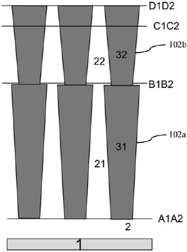
[0153] The difference between the super junction structure of the fourth embodiment of the present invention and the super junction structure of the first embodiment of the present invention is, for example Figure 7A Shown is a device structure diagram of a super-junction device formed by using the super-junction structure of the fourth embodiment of the present invention. The super-junction structure of the fourth embodiment of the present invention includes the following features:
[0154]The second sub-groove 102b is a groove whose top opening is larger than the bottom opening and the sides are inclined, the sides of the first sub-groove 102a are vertical, and the width of the first sub-groove 102a is equal to that of the second sub-groove. By the width of the bottom opening of the groove 102b, the bottom surface of the second sub-trench 102b is aligned with the top surface of the first...
PUM
| Property | Measurement | Unit |
|---|---|---|
| electrical resistivity | aaaaa | aaaaa |
| thickness | aaaaa | aaaaa |
| thickness | aaaaa | aaaaa |
Abstract
Description
Claims
Application Information
 - R&D Engineer
- R&D Manager
- IP Professional
- Industry Leading Data Capabilities
- Powerful AI technology
- Patent DNA Extraction
Browse by: Latest US Patents, China's latest patents, Technical Efficacy Thesaurus, Application Domain, Technology Topic, Popular Technical Reports.
© 2024 PatSnap. All rights reserved.Legal|Privacy policy|Modern Slavery Act Transparency Statement|Sitemap|About US| Contact US: help@patsnap.com