Two-dimensional PLZST antiferroelectric photonic crystal and preparation method thereof

A photonic crystal and antiferroelectric technology, applied in optics, nonlinear optics, instruments, etc., can solve the problems of photonic crystals with many defects, low electron mobility and breakdown field strength, and no obvious changes, and achieve accurate optical parameters , Precise parameters, regular shape effect

Active Publication Date: 2020-06-09
HUBEI UNIV FOR NATITIES
View PDF10 Cites 0 Cited by
  • Summary
  • Abstract
  • Description
  • Claims
  • Application Information

AI Technical Summary

Problems solved by technology

[0004] To sum up, the problems existing in the existing technology are: the photonic crystal structure parameters based on silicon semiconductor materials are precise, but the photonic crystal band gap cannot be adjusted, and it is difficult to be used in the manufacture of tunable optoelectronic integrated devices; Based on metal materials, the structural parameters of ceramic-based photonic crystals prepared by physical and chemical methods are uncontrollable, and the preparation process cannot achieve industrial standardization
[0005] Difficulty in solving the above technical problems: Because silicon is an indirect bandgap semiconductor, it has the disadvantages of low electron mobility and breakdown field strength. There is no significant change in the photonic band gap, which is a defect of the silicon semiconductor material itself
Therefore, silicon semiconductor materials cannot be used to prepare tunable photonic crystals
[0006] Inorganic non-metallic materials can be modified by doping, and show significant sudden changes in lattice constant and dielectric constant under the action of electric field, magnetic field, temperature field, etc., so they have remarkable adjustable characteristics; but photonic crystals are a kind of Artificial metamaterials, whose photoelectric properties are closely related to structural parameters, the structural parameters of inorganic non-metallic photonic crystals prepared by Sol-Gel method, magnetron sputtering method, pulsed laser deposition method, CVD method and other processes are completely uncontrollable. Photonic crystals have too many defects to be industrially produced

Method used


Image

  • Two-dimensional PLZST antiferroelectric photonic crystal and preparation method thereof
  • Two-dimensional PLZST antiferroelectric photonic crystal and preparation method thereof
  • Two-dimensional PLZST antiferroelectric photonic crystal and preparation method thereof

Examples


preparation example Construction

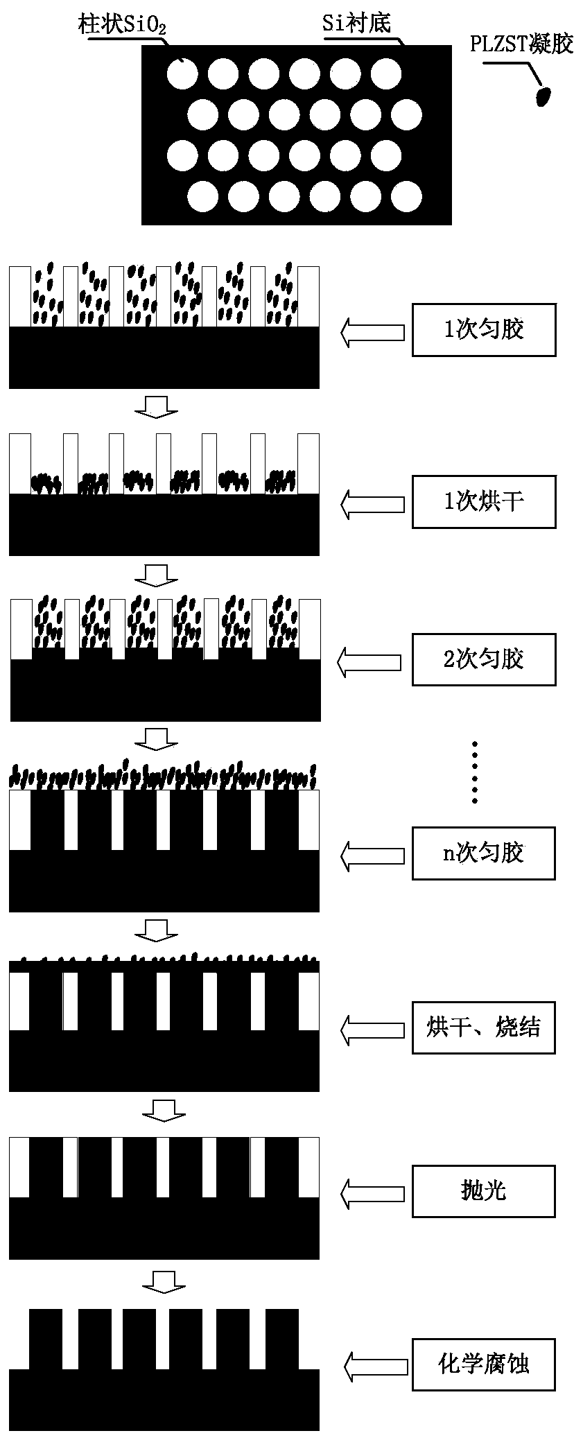
[0039] Such as figure 1 As shown, the two-dimensional PLZST antiferroelectric photonic crystal preparation method provided by the embodiment of the present invention specifically includes:

[0040] (1) Select zirconium n-propoxide, tetrabutyl titanate, lead acetate, tin acetate, lanthanum nitrate, etc. as raw materials, use acetic acid, ethylene glycol ether, acetylacetone, and formamide as solvents, and prepare PLZST by Sol-Gel method Sol.

[0041] (2) Fix the SSO template on the homogenizer, drop PLZST sol, and fill the SSO template by spin coating.

[0042] (3) Heating for the first time on the electric heating plate, the heating temperature is set at 60-80°C, and lasts for 15min at 80°C.

[0043] (4) Fix the sample on the homogenizer after cooling, perform the second spin coating filling, and repeat step (3).

[0044] (5) Repeat step (4) 4 to 5 times.

[0045] (6) Put the sample into a tubular heating furnace, fill it with argon, sinter, and then cool naturally.

[00...

Embodiment

[0060] Such as image 3 As shown, it is a schematic diagram of the preparation method of the two-dimensional PLZST antiferroelectric photonic crystal provided by the embodiment of the present invention.

[0061] Figure 4 It is a schematic diagram of the preparation method of the SSO template provided by the embodiment of the present invention.

[0062] Figure 5 It is a top view of a two-dimensional PLZST antiferroelectric photonic crystal attached to a silicon substrate provided by an embodiment of the present invention.

[0063] In the SEM image of the experimental sample of the present invention, the designed photonic crystal aperture is 500 nanometers. In the case of ignoring the measurement error, the aperture of the photonic crystal air column is almost the same, and the deviation from the experimental design parameters can be ignored. From the perspective of the realization effect, the two-dimensional PLZST photonic crystal prepared by the method provided by the inv...


PUM

PropertyMeasurementUnit
pore sizeaaaaaaaaaa
pore sizeaaaaaaaaaa

Abstract

The invention belongs to the technical field of preparation of electric photon artificial metamaterials, and discloses a two-dimensional PLZST antiferroelectric photonic crystal and a preparation method. The preparation method comprises the following steps: firstly, preparing an SSO template, and then preparing the two-dimensional PLZST antiferroelectric photonic crystal based on the SSO template.The SSO template is prepared by adopting an ICP etching process, the structural parameter error is less than 10nm, the error between the structural parameter and the theoretical design parameter of the prepared two-dimensional PLZST photonic crystal is less than 5nm, and the structural parameter is almost the same as the preset value so that the actually measured optical parameter of the photoniccrystal is more accurate; the PLZST antiferroelectric film is adopted as the dielectric material, PLZST has a remarkable phase change characteristic and an electro-optical effect, specifically, the PLZST antiferroelectric material has the dual effects of lattice constant mutation and dielectric constant shock at a phase change point under the action of the electric field, and the photonic crystalwith the adjustable photonic band gap width is achieved.

Description

technical field [0001] The invention belongs to the technical field of electro-photonic artificial metamaterial preparation, and in particular relates to a two-dimensional PLZST antiferroelectric photonic crystal and a preparation method. Background technique [0002] At present, the closest existing technology is: photonic crystals are a kind of artificially synthesized metamaterials, which have a certain control and manipulation effect on the propagation of light, and have a wide range of applications in the fields of optical communication, optical sensing, and optoelectronic integration. [0003] At present, in order to be compatible with semiconductor electronic materials and preparation processes, research on photonic crystals mainly focuses on silicon semiconductor material systems. However, due to the shortcomings of silicon semiconductor materials such as low electron mobility and breakdown electric field, it is difficult to realize the adjustable bandgap width of ph...

Claims


Application Information

Patent Timeline
Patent Type & Authority Applications(China)
IPC IPC(8): G02F1/05G02F1/03
CPCG02F1/03G02F1/05
Inventor 易金桥孙先波谭建军黄勇胡涛朱黎
Owner HUBEI UNIV FOR NATITIES
Why Eureka
Try Eureka