Mask plate, capacitor array, semiconductor device and preparation method thereof

A capacitor and mask technology, used in semiconductor devices, semiconductor/solid-state device components, electric solid-state devices, etc., can solve problems such as short circuits, DRAM reliability effects, unevenness, etc., and achieve simple process, improved accuracy, and cost. low effect

Pending Publication Date: 2020-04-17
CHANGXIN MEMORY TECH INC
View PDF5 Cites 1 Cited by
  • Summary
  • Abstract
  • Description
  • Claims
  • Application Information

AI Technical Summary

Problems solved by technology

[0006] Additionally, please refer to Figure 2c At present, in order to make the capacitor in the DRAM increase or maintain a sufficiently high capacitance value, the height of the bottom electrode (bottom electrode) 130 in the capacitor is usually increased to increase the contact area between the bottom electrode and the capacitor dielectric layer, and at the same time The stability is also increased by adding a laterally continuous support layer (including the bottom support layer 111, the middle support layer 112 and the top support layer 113) of the electrode, but the lateral support layer will form an uneven boundary of the capacitor array, and the subsequent formation of the conductive contact plug In the plug (CT) 160 process, when the metal conductive material is filled into the contact hole to form the conductive contact plug 160, it is easy to cause cracks (crack) 103 on the sidewall of the contact hole on the periphery of the capacitor array, and the crack 103 may crack to On the uneven boundary of the capacitor array, the metal conductive material filled in the crack will cause a direct short circuit between the conductive contact plug 160 and the boundary of the capacitor array, which will affect the reliability of the DRAM

Method used


Image

  • Mask plate, capacitor array, semiconductor device and preparation method thereof
  • Mask plate, capacitor array, semiconductor device and preparation method thereof
  • Mask plate, capacitor array, semiconductor device and preparation method thereof

Examples


preparation example Construction

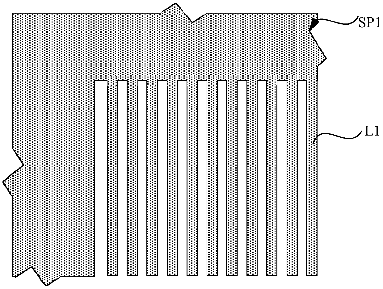
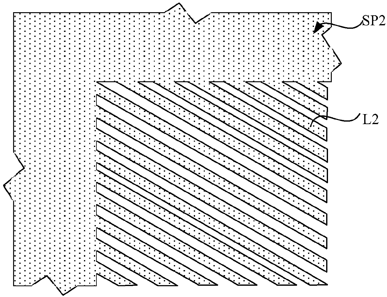
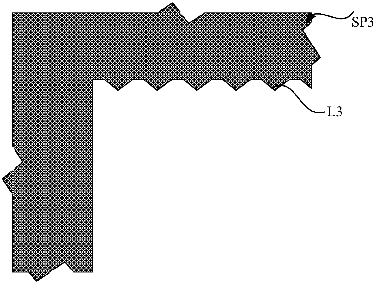
[0128] Please refer to image 3 , an embodiment of the present invention provides a method for preparing a capacitor array, comprising the following steps:

[0129] S1, providing a substrate, forming alternately stacked sacrificial layers and supporting layers on the substrate;

[0130] S2, using the mask plate of the present invention to form a patterned mask layer on the alternately stacked sacrificial layer and support layer through a single exposure process, the patterned mask layer includes a second grid pattern and surrounds A second ring pattern around the second grid pattern, the second grid pattern is interwoven with third lines extending along the first direction and fourth lines extending along the second direction, the second mesh Each second mesh in the grid pattern defines the location of a capacitor, the second annular pattern includes an annular opening immediately surrounding and surrounding the second mesh pattern and surrounding the annular opening away fro...


PUM

PropertyMeasurementUnit
angleaaaaaaaaaa

Abstract

The invention provides a mask plate, a capacitor array, a semiconductor device and a preparation method thereof. A capacitor hole array and an annular groove which surrounds the capacitor hole array and is provided with a wavy side wall can be manufactured through a one-time exposure process; the operation window of the annular groove is large, the situation that etching is not in place can be avoided, and therefore the situation that redundant and small capacitor openings are formed in the boundary of the capacitor array can be prevented, and the reliability of a finally-manufactured device is improved.

Description

technical field [0001] The invention relates to the technical field of semiconductors, in particular to a mask plate, a capacitor array, a semiconductor device and a preparation method thereof. Background technique [0002] Dynamic random access memory (Dynamic Random Access Memory, referred to as: DRAM) is a semiconductor storage device commonly used in computers. It is composed of many repeated storage units. Each storage unit usually includes a capacitor and a transistor. The gate of the transistor is connected to the word line, and the drain The pole is connected to the bit line, and the source is connected to the capacitor; the voltage signal on the word line can control the opening or closing of the transistor, and then read the data information stored in the capacitor through the bit line, or write the data information into the capacitor through the bit line stored in a capacitor. [0003] In the current DRAM manufacturing process, three masks with different patterns...

Claims


Application Information

Patent Timeline
Patent Type & Authority Applications(China)
IPC IPC(8): G03F1/70G03F1/38G03F7/20H01L23/64H01L27/108
CPCG03F1/70G03F1/38G03F7/2045H01L28/40H10B12/30
Inventor 吴晗
Owner CHANGXIN MEMORY TECH INC
Why Eureka
Try Eureka