


Quick Research
Generate reliable direction feasibility study reports for your R&D in just a few steps.

Technical Q&A
Discover and master advanced knowledge NOW. Basics, ideas, possibilities, all at once.

Find Solutions
As an expert in R&D theories, this can generate solutions to your technical problems instantly.

Evaluate Feasibility
Analyze your overall solution with one click, know your potential R&D risks in advance.

Monitor Landscape
Get weekly tech updates, stay abreast of the latest tech innovations and key insights.
MEMS device, manufacturing method thereof and electronic device
An electronic device and device technology, applied in the field of MEMS device and its manufacturing method and electronic device, can solve problems such as pattern layer offset and product failure, and achieve the effects of improving yield, reducing process cost and avoiding alignment offset
- Summary
- Abstract
- Description
- Claims
- Application Information
AI Technical Summary
Problems solved by technology
Method used
Image

Examples
preparation example Construction
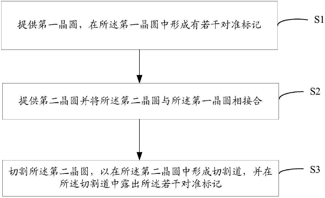
[0038] In order to solve the problems existing in the current technology, the present invention provides a method for preparing a MEMS device, comprising:
[0039] providing a first wafer in which a number of alignment marks are formed;
[0040] providing a second wafer and bonding the second wafer integrally with the first wafer;
[0041] The second wafer is diced to form dicing lines to expose the alignment marks.
[0042] Wherein, a scribe line area is formed in the first wafer, and the alignment mark is formed in the scribe line area.
[0043] The dicing line area in the first wafer corresponds vertically to the dicing line expected to be formed in the second wafer, so as to ensure that the alignment marks can be exposed after dicing the second wafer.
[0044] Wherein, the shape of the alignment mark is not limited to a certain one, and may be a square, a circle, a cross and various easily identifiable patterns.
[0045] Wherein, the number of the alignment marks is not l...
Embodiment 1
[0057] Next, the detailed steps of an exemplary method of the MEMS device manufacturing method proposed by the embodiment of the present invention will be described with reference to the accompanying drawings. in, figure 1 It is a schematic flow chart of a manufacturing method of a MEMS device according to another embodiment of the present invention; Figure 2A-Figure 2C It is a cross-sectional view of a structure formed in the relevant steps of a MEMS device manufacturing method in an embodiment of the present invention.
[0058] Such as figure 1 As shown, a method for manufacturing a MEMS device according to another embodiment of the present invention specifically includes:
[0059] Step S1: providing a first wafer in which several alignment marks are formed;
[0060] Step S2: providing a second wafer and bonding the second wafer to the first wafer;
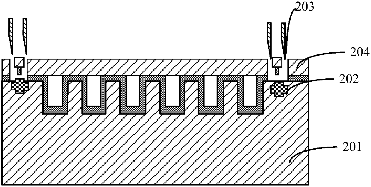
[0061] Step S3: dicing the second wafer to form dicing lines in the second wafer and exposing the alignment marks in the ...
Embodiment 2
[0117] The present invention also provides a MEMS device, which can be prepared by the method of the first embodiment.
[0118] The MEMS devices include:
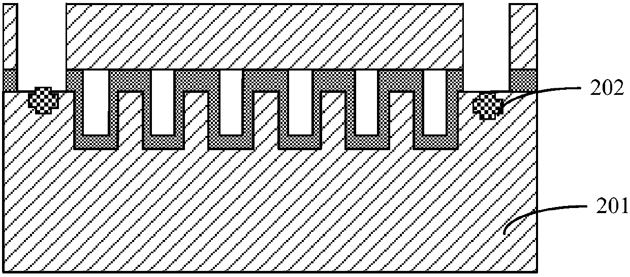
[0119] first wafer 201;
[0120] an alignment mark 202 located in the first wafer;
[0121] The second wafer 204 is bonded to the first wafer 201;
[0122] Wherein, a dicing line 203 is formed in the second wafer 204 to expose the alignment marks in the first wafer.
[0123] Specifically, the first wafer 201 includes at least a semiconductor substrate, and the semiconductor substrate may be at least one of the materials mentioned below: silicon, silicon-on-insulator (SOI), silicon-on-insulator (SSOI) ), silicon germanium on insulator (S-SiGeOI), silicon germanium on insulator (SiGeOI) and germanium on insulator (GeOI), etc.
[0124] In the present invention, the first wafer 201 is made of bare silicon.
[0125] Device patterns are formed on the front surface of the first wafer 201 .
[0126] Specifically, a groove is ...
PUM
 Abstract
Description
Claims
Application Information
 - R&D Engineer
- R&D Manager
- IP Professional
- Industry Leading Data Capabilities
- Powerful AI technology
- Patent DNA Extraction
Browse by: Latest US Patents, China's latest patents, Technical Efficacy Thesaurus, Application Domain, Technology Topic, Popular Technical Reports.
© 2024 PatSnap. All rights reserved.Legal|Privacy policy|Modern Slavery Act Transparency Statement|Sitemap|About US| Contact US: help@patsnap.com