Tunneling field effect transistor and manufacturing method thereof

A tunneling field effect and transistor technology, applied in the field of microelectronics, can solve the problems of random impurity fluctuations of devices, bipolar off-state leakage, device performance degradation, etc., to reduce device power consumption, improve switching speed, and improve reliability. Effect

Active Publication Date: 2020-04-10
XIDIAN UNIV
View PDF4 Cites 0 Cited by
  • Summary
  • Abstract
  • Description
  • Claims
  • Application Information

AI Technical Summary

Problems solved by technology

[0005] 1. Due to the inherent defects in the structure of the device, there is a strong electric field peak at the edge of the gate near the drain when the device is working under negative pressure, which leads to serious bipolar off-state leakage problems
2. The device usually uses traditional ion implantation physical doping technology to achieve device source and drain doping, which will cause random impurity fluctuations in the device
These problems will lead to device performance degradation, reduced reliability, and increased power consumption

Method used


Image

  • Tunneling field effect transistor and manufacturing method thereof
  • Tunneling field effect transistor and manufacturing method thereof
  • Tunneling field effect transistor and manufacturing method thereof

Examples


Embodiment 1

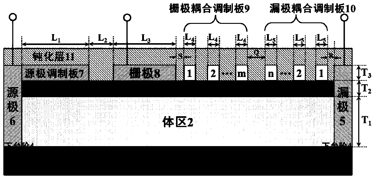
[0061] Embodiment 1: Fabricate a tunneling field effect transistor with one gate sensing plate and one drain sensing plate.

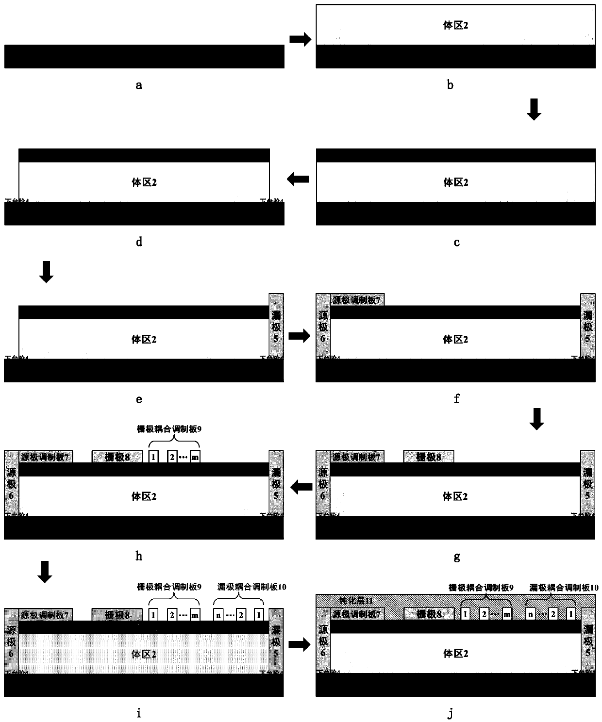
[0062] Step 1. Select silicon semiconductor material as substrate 1, such as image 3 a.

[0063] Step 2. Fabricate the body region 2 on the silicon substrate 1, such as image 3 b.

[0064] A silicon semiconductor material with a thickness of 5 nm is epitaxially grown on a silicon substrate 1 using molecular beam epitaxy technology to form a bulk region 2, wherein the process conditions used for the epitaxy are: the degree of vacuum is less than or equal to 1.0×10 -10 mbar, the RF power is 150W, and the reactant uses high-purity silicon source.

[0065] Step 3. Make gate dielectric layer 3, such as image 3 c.

[0066] A layer of SiN insulating dielectric material with a thickness of 0.5nm is deposited on the upper part of the body region 2 using plasma-enhanced chemical vapor deposition technology, wherein the process conditions for depositing th...

Embodiment 2

[0081] Embodiment 2: Making a Tunneling Field Effect Transistor with 2 Gate Sensing Plates and 2 Drain Sensing Plates

[0082] Step 1. Select InN semiconductor material as substrate 1, such as image 3 a.

[0083] Step 2. Fabricate the body region 2 on the InN substrate 1, such as image 3 b.

[0084] Using molecular beam epitaxy on an InN substrate 1, the vacuum degree is less than or equal to 1.0×10 -10 mbar, the RF power is 150W, and the reactant uses high-purity In source, N 2 The body region 2 is formed by epitaxially epitaxially InN semiconductor material with a thickness of 25 nm under certain process conditions.

[0085] Step 3. Make gate dielectric layer 3, such as image 3 c.

[0086] Use plasma-enhanced chemical vapor deposition technology in the upper part of the body region 2 in the gas NH 3 , N 2 and SiH 4 , the gas flow rate is 2.5sccm, 950sccm and 250sccm, the temperature is 300°C, the RF power is 25W, and the pressure is 950mTorr, a layer of SiN insul...

Embodiment 3

[0105] Embodiment 3: Fabricate a tunneling field effect transistor with three gate sensing plates and three drain sensing plates.

[0106] Step A. select Ge semiconductor material as substrate 1, such as image 3 a.

[0107] Step B. Fabricate body region 2 on Ge substrate 1, such as image 3 b.

[0108] On the Ge substrate 1, a germanium semiconductor material with a thickness of 50nm is epitaxed by using molecular beam epitaxy technology to form the body region 2, wherein the process conditions used for the epitaxy are as follows:

[0109] Vacuum degree is less than or equal to 1.0×10 -10 mbar,

[0110] RF power is 150W,

[0111] The reactant adopts high-purity germanium source.

[0112] Step C. Make gate dielectric layer 3, such as image 3 c.

[0113] A layer of SiN insulating dielectric material with a thickness of 40nm is deposited on the upper part of the body region 2 using plasma enhanced chemical vapor deposition technology, wherein the process conditions for ...


PUM

PropertyMeasurementUnit
widthaaaaaaaaaa
thicknessaaaaaaaaaa
thicknessaaaaaaaaaa

Abstract

The invention discloses a tunneling field effect transistor which mainly aims to solve the problems of random impurity fluctuation and bipolar off-state electric leakage of an existing tunneling fieldeffect transistor. The tunneling field effect transistor is equipped with a substrate (1), a body region (2) and a grid electrode dielectric layer (3) from bottom to top, lower steps (4) are etched at the two sides of the body region and the grid electrode dielectric layer, and a source electrode (6) and a drain electrode (5) are respectively deposited above the lower steps at the left side andthe right side. A source electrode modulation plate (7), a grid electrode (8), and a grid electrode coupling modulation plate (9) and a drain electrode coupling modulation plate (10) which are distributed at an interval are sequentially arranged above the grid dielectric layer from left to right, and a passivation layer (11) is arranged at the periphery of the grid electrode dielectric layer, thedrain, the source, the source modulation plate, the grid electrode , the grid electrode coupling modulation plate and the drain electrode coupling modulation plate. According to the invention, the bipolar off-state electric leakage problem and the random impurity fluctuation problem of the tunneling field effect transistor are solved, the power consumption of the tunneling field effect transistoris reduced, the switching speed and reliability of the tunneling field effect transistor are improved, and the tunneling field effect transistor can be used for a low-power-consumption electronic system.

Description

technical field [0001] The invention belongs to the technical field of microelectronics, and particularly relates to a tunneling field effect transistor, which can be used in a low power consumption circuit system. [0002] technical background [0003] The rapid development of semiconductor technology has promoted the integration level of integrated circuit chips to double every 2 to 3 years, bringing about a huge leap in chip performance. However, with the further reduction of device size, the problem of static power consumption and switching power consumption of traditional MOSFET devices is becoming more and more significant, which cannot fully meet the requirements of future low power consumption applications and energy saving and environmental protection. As a new type of low-power semiconductor device that is expected to replace traditional MOSFET devices, tunneling field-effect transistors (TFETs) are based on quantum band-band tunneling mechanism, which can achieve s...

Claims


Application Information

Patent Timeline
Patent Type & Authority Applications(China)
IPC IPC(8): H01L29/78H01L29/423H01L29/08H01L29/06H01L21/336
CPCH01L29/0634H01L29/0847H01L29/42356H01L29/66568H01L29/78
Inventor 毛维何元浩刘晓雨马佩军杜鸣张进成郝跃
Owner XIDIAN UNIV
Why Eureka
Try Eureka