Tunneling field effect device based on overlapping coupling plate and manufacturing method
A tunneling field effect and coupling plate technology, applied in the field of microelectronics, can solve problems such as reliability decline, power consumption increase, device performance degradation, etc., to suppress bipolar off-state leakage, avoid random impurity fluctuations, and improve device performance. The effect of reliability
- Summary
- Abstract
- Description
- Claims
- Application Information
AI Technical Summary
Problems solved by technology
Method used
Image

Examples
Embodiment 1
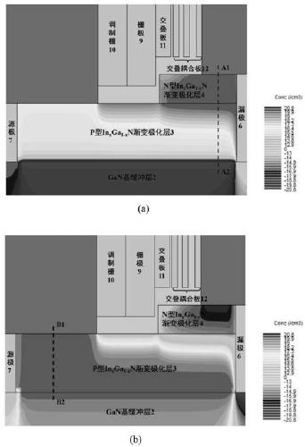
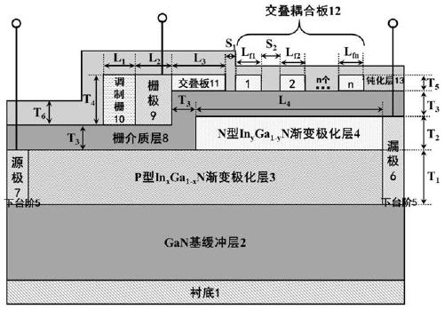
[0051] Embodiment 1: The number of coupling blocks is made to be 1, P-type In x Ga 1-x N graded polarization layer 3 components graded range is x=0.5~0.3, N type In y Ga 1-y A tunneling field effect device based on overlapping coupling plates with 4 components of the N graded polarization layer having a graded range of y=0.1-0.2.
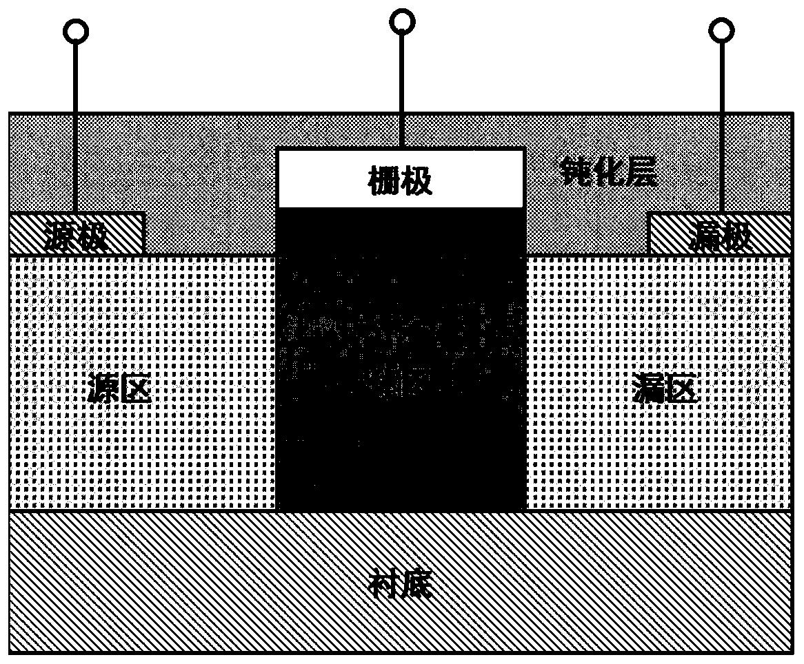
[0052] Step 1. Select silicon semiconductor material as substrate 1, such as image 3 a.
[0053] Step 2. Fabricate a GaN-based buffer layer 2 on the substrate 1, such as image 3 b.
[0054]On the substrate 1, the unintentionally doped GaN semiconductor material with a thickness of 500 nm in the [0001] crystal direction is epitaxially formed by metal-organic chemical vapor deposition technology to form a GaN-based buffer layer 2, wherein the process conditions used for the epitaxy are: the temperature is 950°C, the pressure is 40 Torr, the flow rate of hydrogen gas is 4000 sccm, the flow rate of ammonia gas is 4000 sccm, and the flow rate of ...
Embodiment 2
[0077] Embodiment 2: The number of coupling blocks made is 2, P-type In x Ga 1-x N graded polarization layer 3 components graded range is x=0.5~0.1, N type In y Ga 1-y The N graded polarization layer 4 is a tunneling field effect device based on overlapping coupling plates with a graded range of y=0.1-0.5.
[0078] Step 1. Select sapphire semiconductor material as substrate 1, such as image 3 a.
[0079] Step 2. Fabricate a GaN-based buffer layer 2 on the substrate 1, such as image 3 b.
[0080] Using metal organic chemical vapor deposition technology on the substrate 1 under the process conditions of temperature 950°C, pressure 40Torr, hydrogen gas flow rate 4000 sccm, ammonia gas flow rate 4000 sccm, gallium source flow rate 100μmol / min, the epitaxial thickness is 750nm The GaN semiconductor material is unintentionally doped with the [0001] crystal orientation to form the GaN-based buffer layer 2 .
[0081] Step 3. Make P-type In x Ga 1-x N graded polarization lay...
Embodiment 3
[0103] Embodiment 3: The number of coupling blocks made is 3, P-type In x Ga 1-x N graded polarization layer 3 components graded range is x=1~0, N type In y Ga 1-y The N graded polarization layer 4 is a tunneling field effect device based on overlapping coupling plates with a graded composition range of y=0-0.9.
[0104] Step A. Select silicon carbide semiconductor material as substrate 1, such as image 3 a.
[0105] Step B. Fabricate a GaN-based buffer layer 2 on the substrate 1, such as image 3 b.
[0106] On the substrate 1, the unintentionally doped GaN semiconductor material with a thickness of 1000nm in the [0001] crystal direction is epitaxially formed by metal-organic chemical vapor deposition technology to form a GaN-based buffer layer 2,
[0107] Among them, the process conditions used for epitaxy are:
[0108] The temperature is 950°C, the pressure is 40Torr,
[0109] The hydrogen flow rate is 4000 sccm, the ammonia gas flow rate is 4000 sccm, and the gall...
PUM
| Property | Measurement | Unit |
|---|---|---|
| thickness | aaaaa | aaaaa |
| thickness | aaaaa | aaaaa |
| width | aaaaa | aaaaa |
Abstract
Description
Claims
Application Information
 - Generate Ideas
- Intellectual Property
- Life Sciences
- Materials
- Tech Scout
- Unparalleled Data Quality
- Higher Quality Content
- 60% Fewer Hallucinations
Browse by: Latest US Patents, China's latest patents, Technical Efficacy Thesaurus, Application Domain, Technology Topic, Popular Technical Reports.
© 2025 PatSnap. All rights reserved.Legal|Privacy policy|Modern Slavery Act Transparency Statement|Sitemap|About US| Contact US: help@patsnap.com