Pulse signal amplification method for wide bandgap semiconductor detector

A wide-bandgap semiconductor and pulse signal technology, applied in pulse shaping, single-port active network, etc., can solve the problems of lack of pulse amplification methods for wide-bandgap semiconductor detectors, shorten the pulse shaping period, and reduce the track Loss, the effect of preventing signal distortion

Inactive Publication Date: 2018-06-12
黄仕权
View PDF4 Cites 3 Cited by
  • Summary
  • Abstract
  • Description
  • Claims
  • Application Information

AI Technical Summary

Problems solved by technology

But there is a lack of an effective pulse amplification method for wide bandgap semiconductor detectors

Method used


Image

  • Pulse signal amplification method for wide bandgap semiconductor detector
  • Pulse signal amplification method for wide bandgap semiconductor detector

Examples


Embodiment Construction

[0016] Below in conjunction with accompanying drawing and embodiment the present invention will be further described:

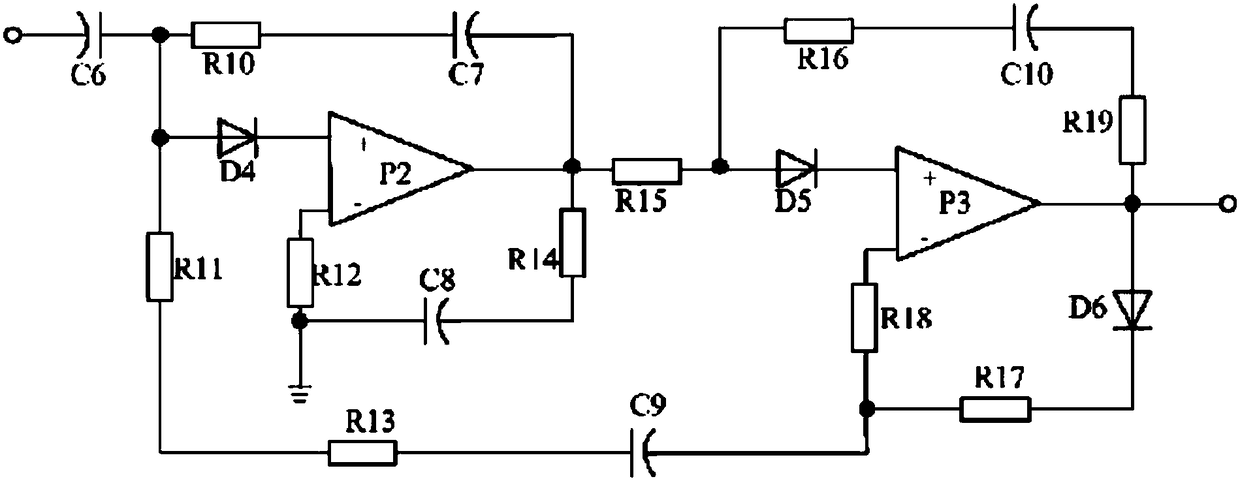
[0017] Such as figure 1 Shown is a pulse amplification method for a wide bandgap II-VI compound semiconductor detector, which includes the following steps:

[0018] First obtain the output signal of the wide-bandgap II-VI compound semiconductor detector, and input the output signal to the impedance matching circuit for impedance matching, and then input it to the band-pass filter circuit for a filter, only allowing the signal The components within the range of the set frequency M1 pass through; secondly, input the aforementioned signal filtered by the band-pass filter into the pole-zero cancellation circuit, and when the signal is narrowed to a certain value through the pole-zero cancellation circuit, the voltage pulse at this time The top of the signal is relatively flat; again, the signal after the pole-zero phase cancellation circuit is input into the uni...


PUM


Abstract

The invention discloses a pulse signal amplification method for a wide bandgap semiconductor detector. The pulse signal amplification method comprises the following steps: first of all, obtaining an output signal of the wide bandgap semiconductor detector, inputting the output signal to perform impedance matching via an impedance matching circuit, and then inputting the output signal into a filtershaping circuit to perform primary filtration, wherein quasi-Gaussian filtering with least levels is adopted by the filter shaping circuit to perform processing on the signal, and only components ina range at a set frequency M1 in the signal are allowed to pass; then, inputting a signal filtered by the filter shaping circuit into a pole-zero cancellation circuit, wherein when the signal is narrowed to a certain value via the pole-zero cancellation circuit, a top portion of a voltage pulse signal is relatively flat; next, inputting a signal after passing through the pole-zero cancellation circuit into a unipolar recovery circuit, so that the signal becomes a unipolar signal; and at last, enabling a signal after passing through the unipolar recovery circuit to pass through a band-pass filter circuit, and then amplifying the signal via an amplification circuit to obtain a final pulse amplification signal. According to the pulse signal amplification method provided by the invention, thepulse amplification signal with an optimal signal-to-noise ratio for the detector can be obtained.

Description

technical field [0001] The invention relates to the field of semiconductor detector signal amplification, in particular to a pulse signal amplification method for wide bandgap semiconductor detectors. Background technique [0002] At present, the electrode output signal of the semiconductor nuclear radiation detector crystal material needs to go through two processes of pre-amplification and shaping amplification. In the traditional nuclear radiation detection electronic circuit, if the pixel array electrode CdZnTe crystal is used for energy spectrum detection, more detection channels mean more signal identification circuits and multi-channel analysis circuits, and the pulse signal of the entire detection system The processing circuit will be very complicated and bulky, so a small-volume high-speed digital processing system with lower cost and higher signal processing rate is usually used at present. Digital signal processing and analysis technology makes the circuit of the...

Claims


Application Information

Patent Timeline
IPC IPC(8): H03K5/02H03H11/46
CPCH03H11/46H03K5/02
Inventor 陈和奎
Owner 黄仕权
Why Eureka
Try Eureka