Eureka AIR delivers breakthrough ideas for toughest innovation challenges, trusted by R&D personnel around the world.

A (100) oriented diamond n-i-p junction diode and its preparation method

An n-i-p, single crystal diamond technology, which is applied in semiconductor/solid-state device manufacturing, semiconductor devices, electrical components, etc., can solve the problems of low quality of i-type layer and high ohmic contact resistivity of n-type layer, etc., to improve the ohmic contact of electrodes traits, reduced spread effects, and quality-enhancing effects

Active Publication Date: 2021-06-04
XI AN JIAOTONG UNIV
View PDF6 Cites 0 Cited by
  • Summary
  • Abstract
  • Description
  • Claims
  • Application Information

AI Technical Summary

Problems solved by technology

[0004] The object of the present invention is to provide a kind of (100) crystal orientation diamond n-i-p junction diode and its preparation method, to solve the problem of high ohmic contact resistivity of n-type layer and low quality of i-type layer in traditional diamond p-i-n junction diode, thereby improving the diamond Performance and Application Prospect of Power Electronic Devices

Method used


Image

  • A (100) oriented diamond n-i-p junction diode and its preparation method
  • A (100) oriented diamond n-i-p junction diode and its preparation method
  • A (100) oriented diamond n-i-p junction diode and its preparation method

Examples


Embodiment 1

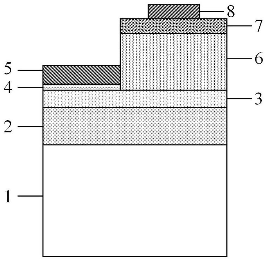
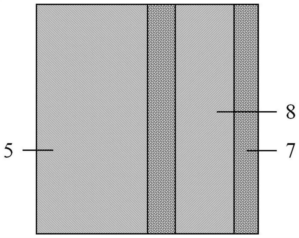
[0041] Such as figure 1 , Ohmic electrical pole rectangular diamond N-I-P diode, the single crystal diamond substrate 1 is high temperature high pressure synthesis single crystal diamond, size is 3 × 3 × 0.3mm 3 . The MPCVD method is used to grow 20 μm n diamond 2 on the surface of the substrate. The growth conditions are: the air pressure is 100 torr, the gas flow is 500 sccm, CH 4 / H2 = 0.05%, pH 3 / CH 4 = 10,000 ppm, substrate temperature is 950 ° C, doping concentration is 10 19 cm -3 . After the growth is over, the n-type diamond 2 is reduced to 10 μm with a polishing polishing machine, and the surface roughness is 1 nm. The MPCVD method is used to grow a layer of N-type diamond thin layer 3 on N-type diamond 2, and the growth conditions are: 100 Torr, gas flow rate of 500 sccm, CH 4 / H 2 = 0.05%, pH 3 / CH 4 = 5000 ppm, the substrate temperature is 900 ° C, and the growth thickness is 10 nm. After the growth, the sample was placed in sulfuric acid and nitric acid 1: 1 mix...

Embodiment 2

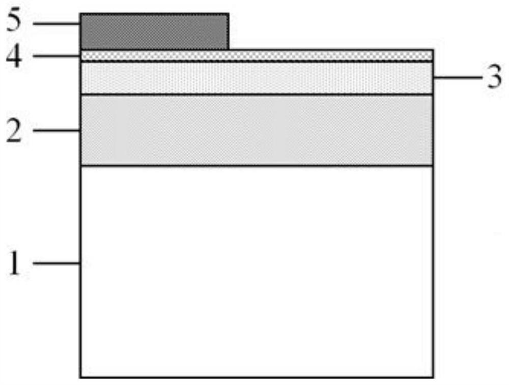
[0043] Such as Figure 4 , Ohmic electrical extremely circular diamond N-I-P diode, the single crystal diamond substrate 1 is high temperature high pressure synthesis single crystal diamond, size of 3 × 3 × 0.3mm 3 . The MPCVD method was used in the surface of the substrate to grow 15 μm n diamond 2, and the growth conditions were: the gas pressure of 100 torr, the gas flow was 500 sccm, CH 4 / H 2 = 0.05%, pH 3 / CH 4 = 10,000 ppm, substrate temperature is 950 ° C, doping concentration is 10 19 cm -3 . After the growth is over, the n-type diamond 2 is reduced to 5 μm with a polishing polishing machine, and the surface roughness is 0.5 nm. The MPCVD method is used to grow a layer of N-type diamond thin layer 3 on N-type diamond 2, and the growth conditions are: 100 Torr, gas flow rate of 500 sccm, CH 4 / H 2 = 0.05%, pH 3 / CH 4 = 100000 ppm, the substrate temperature is 900 ° C, and the growth thickness is 20 nm. After the growth is over, the sample is treated with ultraviolet ozo...


PUM

PropertyMeasurementUnit
thicknessaaaaaaaaaa
surface roughnessaaaaaaaaaa
thicknessaaaaaaaaaa

Abstract

The invention discloses a (100) crystal orientation diamond n-i-p junction diode and a preparation method thereof, which solves the problems of large n-type layer ohmic contact resistivity and low i-type layer quality in traditional diamond p-i-n junction diodes. problems, thereby improving the performance and application prospects of diamond power electronic devices. A (100) crystal orientation diamond n-i-p junction diode, the specific structure of which is: (100) crystal orientation intrinsic single crystal diamond substrate, n-type diamond and n-type diamond thin layer stacked from bottom to top ; On the n-type diamond thin layer: one part is a highly conductive surface and ohmic electrode I that are stacked from bottom to top, and the other part is i-type diamond, p-type diamond, and ohmic electrode II that are stacked from bottom to top.

Description

【Technical field】 [0001] The invention belongs to the technical field of semiconductor devices, and specifically relates to a (100) crystal orientation diamond n-i-p junction diode and a preparation method thereof. 【Background technique】 [0002] In the past decade, diamond switching devices have mainly been Schottky diodes based on Schottky junctions. In general, Schottky junction devices are attractive unipolar devices due to their fast switching speed and relatively low on-state voltage drop. However, in the field of ultra-high voltage devices, p-i-n junction diodes have more advantages because the thickness of their intrinsic layer (i layer) can support high voltages. As part of power electronic devices, p-i-n diodes are made by adding a low-doped intrinsic semiconductor layer between p-type and n-type semiconductor materials and have a wide range of applications from low to high frequencies. However, due to the immature n-type doping technology of diamond semiconducto...

Claims


Application Information

Patent Timeline
Patent Type & Authority Patents(China)
IPC IPC(8): H01L29/868H01L21/328
CPCH01L29/6609H01L29/66121H01L29/868
Inventor 王宏兴刘璋成赵丹王娟邵国庆易文扬李奇王玮问峰
Owner XI AN JIAOTONG UNIV
Why Eureka
Eureka Blog
Learn More