Nanometer metal film auxiliary substrate and fabrication method thereof
A nano-metal film and auxiliary substrate technology, applied in the direction of nanotechnology, nanotechnology, nanotechnology for materials and surface science, etc., can solve the problems of high porosity, high sintering temperature, poor thermal conductivity, etc., to achieve improved Reliability, the effect of lowering the firing temperature
- Summary
- Abstract
- Description
- Claims
- Application Information
AI Technical Summary
Problems solved by technology
Method used
Image
Examples
Embodiment 1
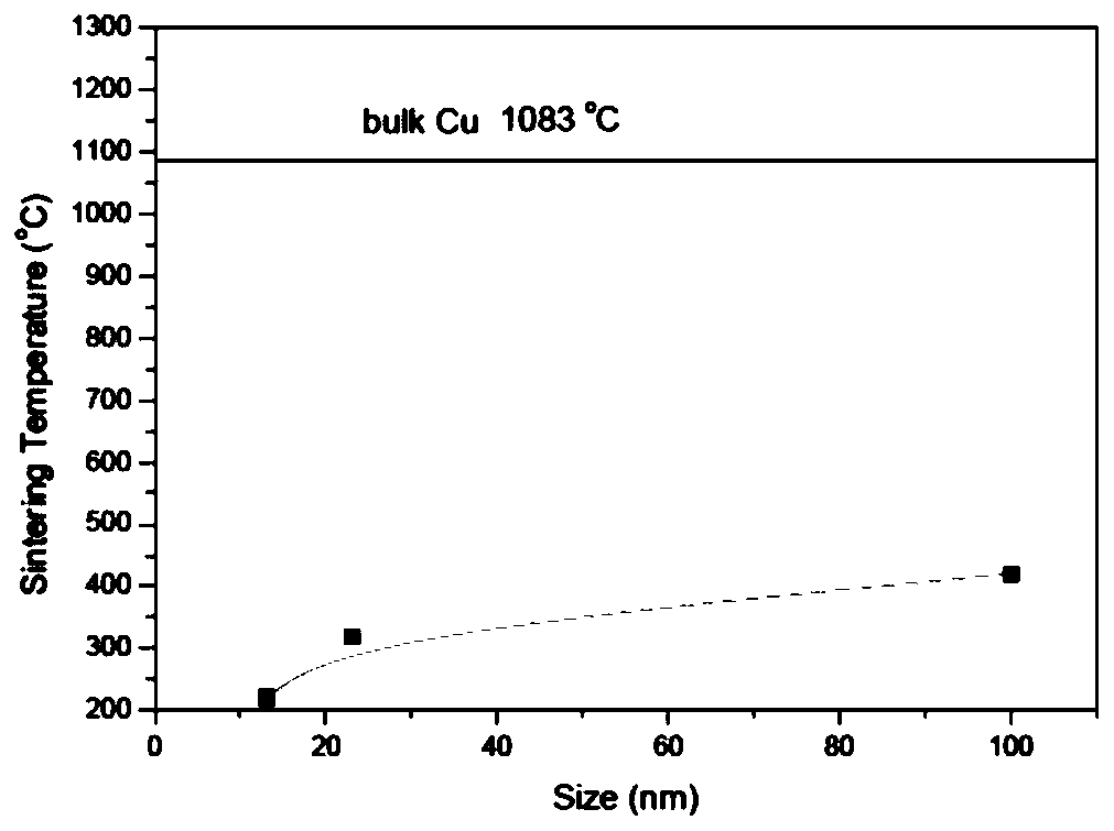
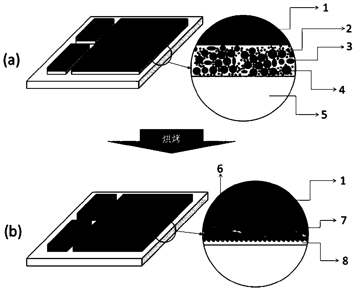
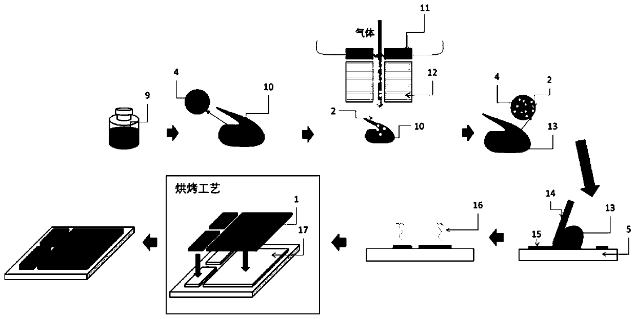
[0057] This embodiment provides the relationship between the nano copper shell and the sintering temperature, the structure described in this embodiment, such as figure 2 As shown in (a), it is characterized in that the main body (first material) connecting the auxiliary layer is silver-copper-titanium active brazing material, and the second material is nano-copper particles, which are driven into the main body of the first material solder by physical impact, The ceramic material is silicon nitride, and the solder is placed on the surface of the ceramic substrate by screen printing, and the final metal-ceramic substrate is formed by baking the system, such as figure 2 (b) shown.
Embodiment 2
[0059] This embodiment provides a schematic structural view of a cermet substrate with a nano-metal auxiliary layer. The structure described in this embodiment is characterized in that the main body (the first material) connecting the auxiliary layer is silver copper titanium active brazing material. The second material is a nano-tin material, which is penetrated into the main body of the first material solder by physical impact to form a coating on the titanium element in the active solder; titanium is easy to oxidize and deactivate during the baking process, so high vacuum conditions are extremely important ; Through tin coating, it can effectively resist oxidation, thereby reducing the dependence on vacuum conditions.
Embodiment 3
[0061] This embodiment provides a nano-metal film auxiliary substrate structure, such as figure 2 shown. The structure described in this embodiment is characterized in that the main body (first material) of the connection auxiliary layer and the second material driven in are both copper materials, so when connecting the oxygen-free copper and the ceramic substrate, the connection layer and the copper foil Copper-copper bonding can be achieved between them to improve the connection strength. before baking, such as figure 2 As shown in (a), there is an unformed connection auxiliary layer material between the oxygen-free copper foil 1 and the ceramic substrate 5, which includes large-sized copper particles 4 with an average particle diameter of 0.1-100 μm, and small copper particles with an average particle diameter of 1 nm-100 nm. Nano-sized copper particles 2, glass or ceramic phase composed of bismuth oxide, silicon oxide, aluminum oxide, calcium oxide, sodium oxide, cesiu...
PUM
| Property | Measurement | Unit |
|---|---|---|
| Diameter | aaaaa | aaaaa |
| Diameter | aaaaa | aaaaa |
| The average particle size | aaaaa | aaaaa |
Abstract
Description
Claims
Application Information
 - R&D Engineer
- R&D Manager
- IP Professional
- Industry Leading Data Capabilities
- Powerful AI technology
- Patent DNA Extraction
Browse by: Latest US Patents, China's latest patents, Technical Efficacy Thesaurus, Application Domain, Technology Topic, Popular Technical Reports.
© 2024 PatSnap. All rights reserved.Legal|Privacy policy|Modern Slavery Act Transparency Statement|Sitemap|About US| Contact US: help@patsnap.com


