Phosphor, method for preparing phosphor, optoelectronic component, and method for producing optoelectronic component
A technology of optoelectronic devices and fluorescent materials, applied in the manufacturing process of optoelectronic devices, the field of optoelectronic devices
- Summary
- Abstract
- Description
- Claims
- Application Information
AI Technical Summary
Problems solved by technology
Method used
Image
Examples
Embodiment 1
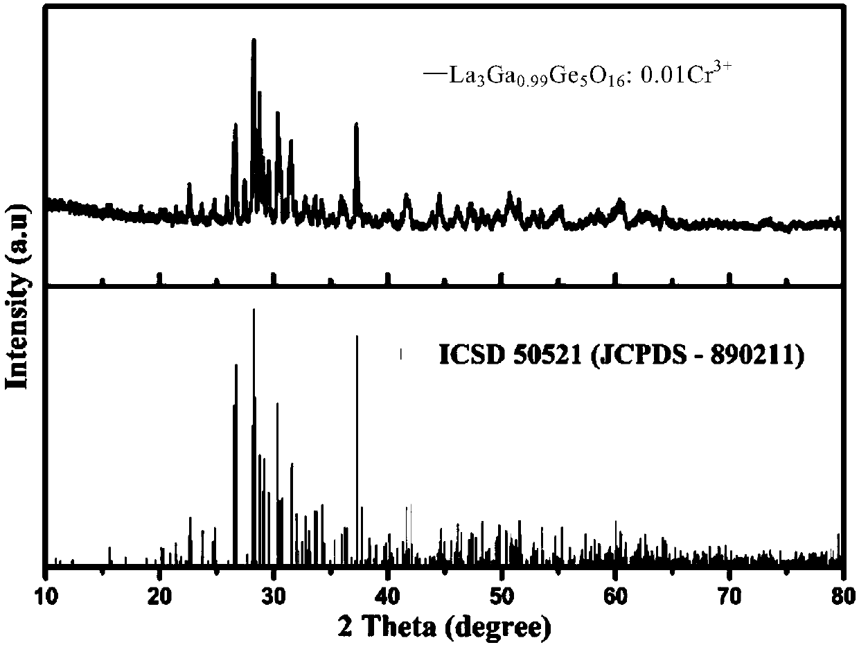
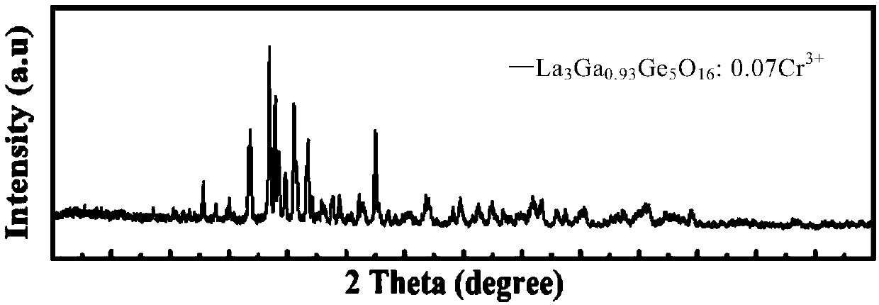
[0091] This embodiment provides a group of fluorescent materials whose general formula is La 3 Ga 1-y Ge 5 o 16 :yCr 3+ , where 0<y≤0.2, the chemical formula of this group of fluorescent materials is as follows:
[0092] La 3 Ga 0.995 Ge 5 o 16 :0.005Cr 3+
[0093] La 3 Ga 0.99 Ge 5 o 16 :0.01Cr 3+
[0094] La 3 Ga 0.97 Ge 5 o 16 :0.03Cr 3+
[0095] La 3 Ga 0.95 Ge 5 o 16 :0.05Cr 3+
[0096] La 3 Ga 0.93 Ge 5 o 16 :0.07Cr 3+
[0097] La 3 Ga 0.91 Ge 5 o 16 :0.09Cr 3+
[0098] La 3 Ga 0.89 Ge 5 o 16 :0.11Cr 3+
[0099] La 3 Ga 0.87 Ge 5 o 16 :0.13Cr 3+
[0100] The preparation method of this group of fluorescent materials is: according to the stoichiometric ratio in the molecular formula of the fluorescent materials, accurately weigh the raw material La 2 o 3 , Ga 2 o 3 、GeO 2 and Cr 2 o 3 ;Put the weighed raw materials into an agate mortar and grind to mix evenly, then transfer the resulting mixture to an alumina crucibl...
Embodiment 2
[0105] This embodiment provides a fluorescent material with a molecular formula of La 2.97 Ga 0.99 Ge 5 o 16 :0.03Gd 3+ ,0.01Cr 3+ , the preparation method of the fluorescent material is as follows:
[0106] Accurately weigh the raw material La according to the stoichiometric ratio in the molecular formula of the fluorescent material 2 o 3 , Ga 2 o 3 、GeO 2 、Gd 2 o 3 and Cr 2 o 3 , put the weighed raw material into an agate mortar and grind it to mix evenly, then transfer the mixture to an alumina crucible, and place it in a tube furnace for sintering in an air atmosphere, controlling the sintering temperature to 1300°C The sintering time is about 6 hours, and after being cooled in the furnace, it is ground into powder to obtain fluorescent materials.
[0107] Such as Figure 5 As shown, the XRD diffraction pattern of the fluorescent material is compared with the standard X-ray diffraction pattern, and all the diffraction peaks of the fluorescent material are co...
Embodiment 3
[0111] This embodiment provides a fluorescent material whose molecular formula is La 2.97 Ga 0.99 Ge 5 o 16 :0.03Yb 3+ ,0.01Cr 3+ , the preparation method of the fluorescent material is as follows:
[0112] Accurately weigh the raw material La according to the stoichiometric ratio in the molecular formula of the fluorescent material 2 o 3 , Ga 2 o 3 、GeO 2 , Yb 2 o 3 and Cr 2 o 3 , put the weighed raw material into an agate mortar and grind it to mix evenly, then transfer the mixture to an alumina crucible, and place it in a tube furnace for sintering in an air atmosphere, controlling the sintering temperature to 1300°C The sintering time is about 6 hours, and after being cooled in the furnace, it is ground into powder to obtain fluorescent materials.
[0113] Such as Figure 7 As shown, the XRD diffraction pattern of the fluorescent material is compared with the standard X-ray diffraction pattern, and all the diffraction peaks of the fluorescent material are co...
PUM
 Abstract
Description
Claims
Application Information
 - R&D Engineer
- R&D Manager
- IP Professional
- Industry Leading Data Capabilities
- Powerful AI technology
- Patent DNA Extraction
Browse by: Latest US Patents, China's latest patents, Technical Efficacy Thesaurus, Application Domain, Technology Topic, Popular Technical Reports.
© 2024 PatSnap. All rights reserved.Legal|Privacy policy|Modern Slavery Act Transparency Statement|Sitemap|About US| Contact US: help@patsnap.com


