
Organic light-emitting diode panel and manufacturing method thereof

A technology of light-emitting diodes and manufacturing methods, which is applied in semiconductor/solid-state device manufacturing, electrical components, electric solid-state devices, etc., and can solve the problem of loss of functionality of the panel

Inactive Publication Date: 2019-06-11
WUHAN CHINA STAR OPTOELECTRONICS SEMICON DISPLAY TECH CO LTD
View PDF4 Cites 13 Cited by
  • Summary
  • Abstract
  • Description
  • Claims
  • Application Information

AI Technical Summary

Problems solved by technology

refer to Figure 1B Although the devices and wiring of the thin film transistor array layer 30 inside the panel can be avoided, the light-emitting organic film layer 40 (including the hole injection layer, the hole transport layer, the light emitting layer, the electron transport layer, the electron injection layer, Cathode layer, etc.) is generated by Open Mask evaporation. After O-shaped cutting, the cross-section of the cutting edge will be exposed, so water vapor (dotted arrow) will infiltrate from this position, and the panel will lose its functionality.

Method used


Image

  • Organic light-emitting diode panel and manufacturing method thereof
  • Organic light-emitting diode panel and manufacturing method thereof
  • Organic light-emitting diode panel and manufacturing method thereof

Examples


Embodiment Construction

[0022] The following descriptions of the various embodiments refer to the accompanying drawings to illustrate specific embodiments in which the invention may be practiced. Furthermore, the directional terms mentioned in the present invention, such as up, down, top, bottom, front, rear, left, right, inner, outer, side, surrounding, center, horizontal, lateral, vertical, longitudinal, axial, Radial, uppermost or lowermost, etc., are only directions with reference to the attached drawings. Therefore, the directional terms used are for describing and understanding the present invention, not for limiting the present invention.

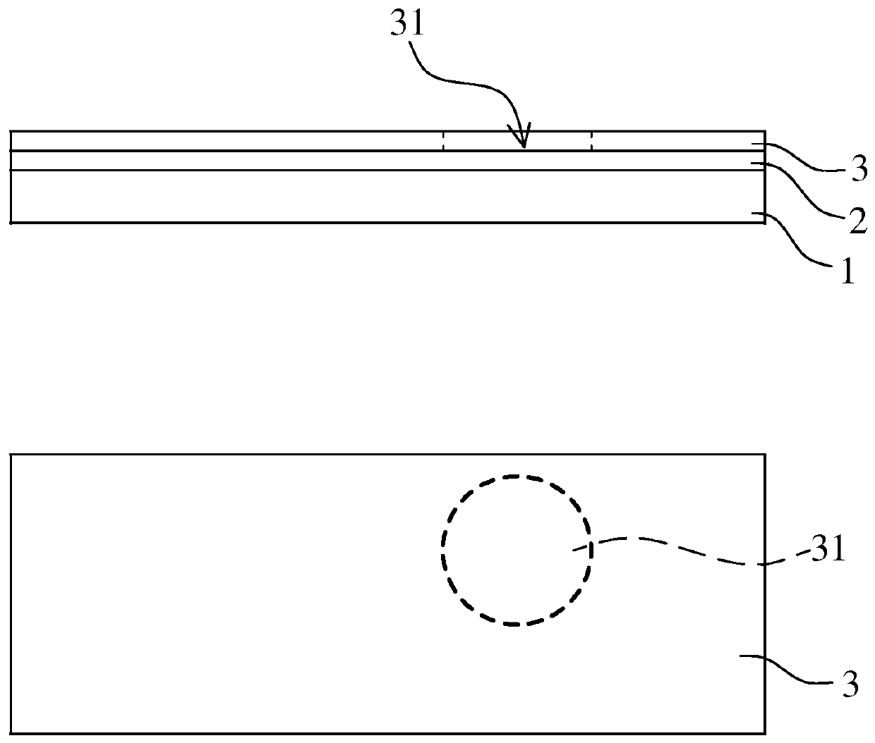
[0023] Please refer to Figures 2A to 2E , which shows a brief flow of a method for manufacturing an organic light-emitting diode panel of the present invention, wherein Figures 2A to 2E Each figure contains a corresponding side view (above) and a top view (below).

[0024] like Figure 2A As shown, in this step, a carrier substrate 1 is provided, and ...


PUM


Abstract

The invention discloses an organic light-emitting diode panel and a manufacturing method thereof. The manufacturing method comprises the following steps of (1) sequentially forming a thin film transistor array functional layer and an organic light-emitting layer on a flexible and transparent substrate, wherein the thin film transistor array functional layer is provided with a predetermined removalregion; (2) removing the organic light-emitting layer above the predetermined removal region by first laser so as to form a groove; (3) covering the organic light-emitting layer and the groove with apackage layer; and (4) cutting the package layer arranged in the groove and the flexible and transparent substrate by second laser to form an opening hole.

Description

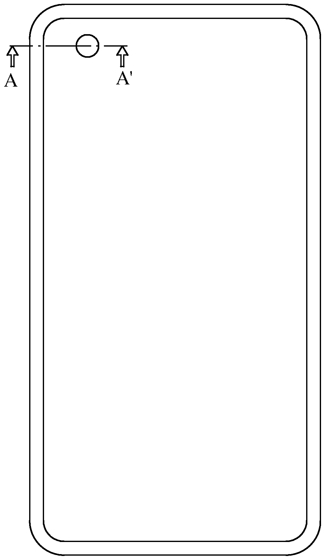
technical field [0001] The present invention relates to an organic light emitting diode panel and a manufacturing method thereof, in particular, to an organic light emitting diode panel and a manufacturing method thereof that can avoid the intrusion of water vapor. Background technique [0002] With the continuous development of science and technology, people's requirements for display devices are getting higher and higher. As is known to all, organic light emitting diode (OLED) display devices have received extensive attention due to their narrow borders, light weight, rollability, and easy portability. [0003] Nowadays, the design of "full screen" has become the mainstream, and major manufacturers are focusing on the research and development of full screen products with a high screen ratio. The recent rise of "O-Cut" design (please refer to Figure 1A ), that is, a circular through hole is dug directly on the panel to place the front camera, which can be closer to the fu...

Claims


Application Information

Patent Timeline
Patent Type & Authority Applications(China)
IPC IPC(8): H01L27/32H01L51/00H01L51/52H10K99/00
Inventor 孙亮曾勉王硕晟李雪
Owner WUHAN CHINA STAR OPTOELECTRONICS SEMICON DISPLAY TECH CO LTD
Learn More