
Graphene preparation method based on microwave plasma chemical vapor deposition

A microwave plasma and chemical vapor deposition technology, which is applied in gaseous chemical plating, semiconductor/solid-state device manufacturing, electrical components, etc., can solve the problems of high graphene growth temperature, lower graphene quality, stress and topological defects, etc. Achieve the effects of reducing thermal stress, controllable preparation, and shortening reaction time

Active Publication Date: 2019-06-07
INST OF SEMICONDUCTORS - CHINESE ACAD OF SCI
View PDF6 Cites 6 Cited by
  • Summary
  • Abstract
  • Description
  • Claims
  • Application Information

AI Technical Summary

Problems solved by technology

Although the method of combining internal and external carbon sources in the prior art avoids the problems of the two common methods to a certain extent, the method needs to deposit metal during the growth process and remove the metal by etching after the growth, and the process is relatively complicated.
Although Michon and Strupinski et al. used hot wall CVD to directly prepare graphene on SiC, the growth temperature of graphene is relatively high, which may reduce the quality of graphene, such as introducing stress and topological defects.

Method used


Image

  • Graphene preparation method based on microwave plasma chemical vapor deposition
  • Graphene preparation method based on microwave plasma chemical vapor deposition
  • Graphene preparation method based on microwave plasma chemical vapor deposition

Examples


preparation example Construction

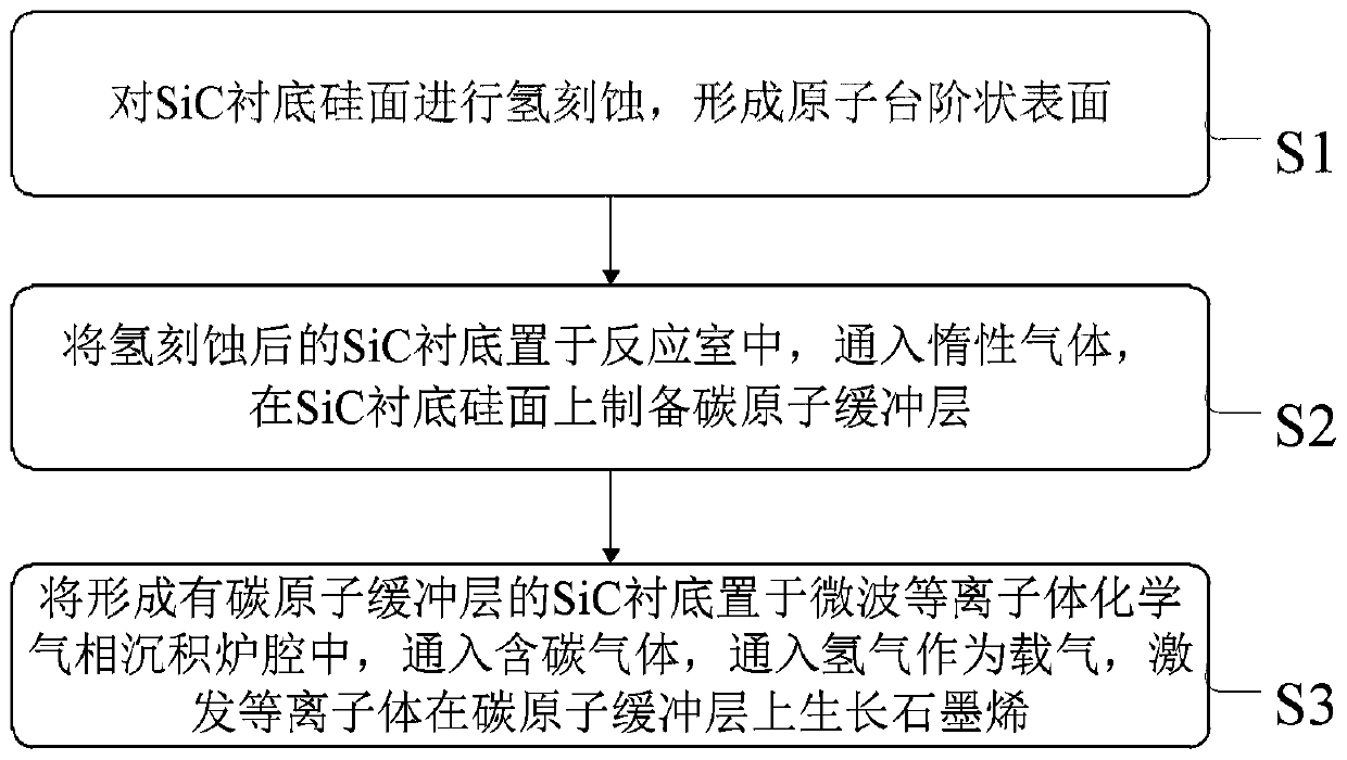
[0032] figure 1 Show the graphene preparation method flowchart based on microwave plasma chemical vapor deposition of the present invention, as figure 1 As shown, the methods include:

[0033] S1, performing hydrogen etching on the silicon surface of the SiC substrate to form an atomically stepped surface.

[0034] The silicon surface of the SiC substrate is etched with hydrogen by using a high-temperature annealing furnace or a microwave plasma chemical vapor deposition growth furnace. When using a high-temperature annealing furnace to perform hydrogen etching on the silicon surface of the SiC substrate, raise the temperature to 1200-1800°C and etch for 10-60 minutes; use a microwave plasma chemical vapor deposition growth furnace to perform hydrogen etching on the silicon surface of the SiC substrate During etching, the temperature is raised to 600-1000° C. and etched for 10-60 minutes. In the hydrogen etching process of SiC, high-purity hydrogen or a mixture of high-puri...

Embodiment 1

[0043] The method for preparing graphene on SiC substrate in the present embodiment comprises the following steps:

[0044] First, the surface treatment of the SiC substrate. Specifically, the SiC substrate is placed in a high-temperature annealing furnace, a pure hydrogen atmosphere is selected during the etching process, the chamber pressure is 600 Torr, and the treatment is performed at 1400° C. for 10 minutes. After hydrogen treatment, surface scratches can be removed and a substrate surface with regular atomic steps can be formed.

[0045] Then, a carbon atom buffer layer is prepared. Specifically, the SiC substrate after surface treatment is placed in a reaction chamber, and a high-purity argon atmosphere is selected as the gas. The carbon atom buffer layer can be obtained by growing at 1400°C and 600 Torr gas pressure for 10 minutes, and due to the low temperature, pyrolytic graphene will not be formed at this time.

[0046] Finally, epitaxially grow graphene on the ...

Embodiment 2

[0048] The difference between this embodiment and Implementation 1 is that the hydrogen etching method of the substrate is different, the graphene growth time is prolonged, and a graphene sample with more layers is obtained, which specifically includes the following steps:

[0049] First, the surface treatment of the SiC substrate. Specifically, the SiC substrate is placed in an MPCVD growth furnace, and a pure hydrogen atmosphere is selected during the etching process under the conditions of a pressure of 80 Torr and a temperature of 800° C. for 10 minutes. After hydrogen treatment, surface scratches can be removed and a substrate surface with regular atomic steps can be formed.

[0050] Then, a carbon atom buffer layer is prepared. Specifically, the SiC substrate after surface treatment is placed in a reaction chamber, and the gas is selected as pure argon atmosphere. The carbon atom buffer layer can be obtained by growing at 1400°C and 600 Torr gas pressure for 10 minutes...


PUM


Abstract

The invention provides a graphene preparation method. The graphene preparation method comprises the steps that hydrogen etching is carried out on a SiC substrate silicon face to form an atom step-shaped surface; a SiC substrate subjected to hydrogen etching is arranged in a reaction chamber, inert gas is fed into the reaction chamber, and a carbon atom buffer layer is prepared on the SiC substratesilicon face; and the SiC substrate on which the carbon atom buffer layer is formed is arranged in a microwave plasma chemical vapor deposition furnace chamber, carbon gas is fed with hydrogen serving as carrier gas, and plasma is stimulated to grow graphene on the buffer layer. The graphene prepared through the method can be directly manufactured into a device without transferring or following treatment, and device preparation is facilitated; by means of the application of the plasma, the thermal stress caused by a reaction temperature and the high temperature is reduced, preparation of thegraphene is more controllable, application of the graphene device is facilitated, the reaction time is effectively shortened, and the reaction rate is accelerated; and the carbon atom buffer layer serves as a middle layer, the defect that in a pyrolysis method, the migration rate of the graphene is reduced by the buffer layer is avoided, and the graphene quality is optimized.

Description

technical field [0001] The invention relates to the technical field of semiconductor thin film materials, in particular to a method for preparing graphene based on microwave plasma chemical vapor deposition. Background technique [0002] Graphene is composed of single layer sp 2 A new type of two-dimensional material composed of carbon atoms with a hexagonal honeycomb lattice structure, which has excellent electrical, thermal, and mechanical properties, is expected to be widely used in ultra-high-speed computer chips, optoelectronic devices, sensors, fuel cells, etc. It is considered to be one of the candidate materials for microelectronic technology to replace silicon in the post-CMOS era. In order to realize the expected application of graphene, the preparation of high-quality graphene wafers is very important. [0003] There are two main methods for the preparation of graphene, one is SiC pyrolysis, and the other is CVD. The SiC pyrolysis method releases silicon atoms ...

Claims


Application Information

Patent Timeline
Patent Type & Authority Applications(China)
IPC IPC(8): C23C16/26C23C16/511C23C16/513C23C16/517H01L21/02
Inventor 郁万成金鹏王占国
Owner INST OF SEMICONDUCTORS - CHINESE ACAD OF SCI
Learn More