Graphene transparent electrode and work function regulation and control method thereof
A transparent electrode and graphene technology, applied in the field of materials, can solve problems such as the inability to meet the requirements of the work function of OLED device electrodes, and achieve good stability
- Summary
- Abstract
- Description
- Claims
- Application Information
AI Technical Summary
Problems solved by technology
Method used
Image
Examples
Embodiment 1
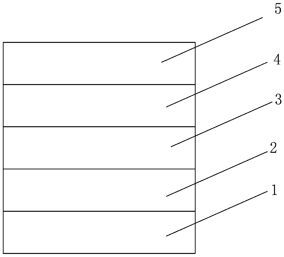
[0028] Such as figure 1 Shown, is the structural representation of graphene transparent electrode among the present invention, a kind of graphene transparent electrode, comprises the transparent base material 1, ultra-thin copper layer 2, graphene layer 3, metal thin film layer 4 that are connected successively; The transparent An ultra-thin copper layer 2 is plated on the base material 1; a graphene layer 3 is formed on the surface of the ultra-thin copper layer 2; a metal film layer 4 is deposited on the surface of the graphene layer 3. An anti-reflection and anti-reflection layer 5 is deposited on the surface of the metal thin film layer 4 .
[0029] The transparent substrate 1 is any one of glass, quartz, sapphire, polyethylene terephthalate PET, polyimide PI, and polyethylene naphthalate PEN.
[0030] The thickness of the ultra-thin copper layer 2 is 1-20 nm, and the thickness of the ultra-thin copper layer is higher than the surface roughness of the transparent substrat...
Embodiment 2
[0033] A method for regulating the work function of a graphene transparent electrode, comprising the steps of:
[0034] Step 1, pretreating the transparent substrate 1 .
[0035] In step 2, an ultra-thin copper layer 2 with a thickness of 10 nm is plated on the transparent substrate 1, which is beneficial for the subsequent generation of the graphene layer 3 without transfer.
[0036] Step 3, put the transparent substrate 1 coated with the ultra-thin copper layer 2 into the chamber of the CVD furnace; feed the carrier gas H2, heat up to the graphene growth temperature of 980°C, and feed the carbon source gas CH4 into the CVD chamber , CH4 gas nucleates on the copper surface to form a graphene layer 3; after the growth is completed, stop feeding CH4 gas and continue feeding carrier gas H2. Layer 2, sample of transparent substrate 1.
[0037] Step 4, depositing a metal thin film layer 4 on the graphene layer 3, and the following conditions are met: a negative potential is appl...
Embodiment 3
[0041] A method for regulating the work function of a graphene transparent electrode, comprising the steps of:
[0042] Step 1, pretreating the transparent substrate 1 .
[0043] In step 2, an ultra-thin copper layer 2 with a thickness of 10 nm is plated on the transparent substrate 1, which is beneficial for the subsequent generation of the graphene layer 3 without transfer.
[0044] Step 3, put the transparent substrate 1 coated with the ultra-thin copper layer 2 into the chamber of the CVD furnace; feed the carrier gas H2, heat up to the graphene growth temperature of 980°C, and feed the carbon source gas CH4 into the CVD chamber , CH4 gas nucleates on the surface of the ultra-thin copper layer 2 to form a graphene layer 3; after the growth of the graphene layer 3 is completed, stop feeding CH4 gas and continue feeding carrier gas H2 until the chamber drops to room temperature, Take out a sample composed of graphene layer 3, ultra-thin copper layer 2, and transparent subst...
PUM
| Property | Measurement | Unit |
|---|---|---|
| Thickness | aaaaa | aaaaa |
| Thickness | aaaaa | aaaaa |
Abstract
Description
Claims
Application Information
 - Generate Ideas
- Intellectual Property
- Life Sciences
- Materials
- Tech Scout
- Unparalleled Data Quality
- Higher Quality Content
- 60% Fewer Hallucinations
Browse by: Latest US Patents, China's latest patents, Technical Efficacy Thesaurus, Application Domain, Technology Topic, Popular Technical Reports.
© 2025 PatSnap. All rights reserved.Legal|Privacy policy|Modern Slavery Act Transparency Statement|Sitemap|About US| Contact US: help@patsnap.com

