
Method and device for detecting blind hole of circuit board

A detection method and technology of detection equipment, which are used in electronic circuit testing, electrical measurement, measurement devices, etc., can solve the problems of local contact, expensive buried holes, and poor bonding between the bottom of the blind hole and the inner layer of copper. The effect of reduced quality and simple and effective testing methods

Inactive Publication Date: 2019-02-15
昆山中哲电子有限公司
View PDF2 Cites 2 Cited by
  • Summary
  • Abstract
  • Description
  • Claims
  • Application Information

AI Technical Summary

Problems solved by technology

[0003] Micro vias are mainly divided into three categories, namely: blind vias, buried vias and plated through-holes (PTH), which are used to achieve electrical interconnection between layers of multilayer PCBs. , although the plated through hole is cheap, it will take up some PCB space, the buried hole is expensive and the process is complicated, and the blind hole is widely used because it can make full use of the PCB space and the manufacturing process is simple.
[0004] The electroplating blind hole process mainly includes: laser, cleaning, glue removal, copper sinking, hole filling electroplating, etc. The performance and reliability of the blind hole coating will be affected by each step of the process, and defects or negligence in any link will have The performance of plated blind holes may not meet the standard, resulting in poor bonding between the bottom of the blind hole and the inner layer copper after hole filling and electroplating, and eventually cause open circuit, short circuit and other faults on the PCB and cannot be used normally, resulting in large economic losses
At present, the commonly used method of detecting blind holes is mainly through the blind hole daisy chain on the manufacturing process for random testing. Only when the hole is broken and the ICD contact is completely disconnected can it be found, otherwise the process control cannot detect it, and it is for the part of the shipment inspection. At present, the 100% power-on test is mainly carried out through electrical testing, and the defect mode of a broken hole or a bad ICD is not completely disconnected but has partial contact. The power-on inspection test in the factory does not find abnormalities, which leads to abnormal boards flowing out. When the client uploads the software, it cracks after the customer uploads the software at high temperature, causing the function to fail or the customer opens the circuit after using it for a period of time, resulting in the failure of the product function. Most of the control methods for the high-density interconnection industry use the mechanism of measuring daisy chains and electrical testing. In view of some large manufacturers’ stuck control in the process, AOI inspection after electroplating and degumming and four-line random testing of finished products will be added. This kind of investment is relatively large and can reduce the frequency of abnormalities. To avoid some problems, blind holes cannot be detected after electroplating

Method used

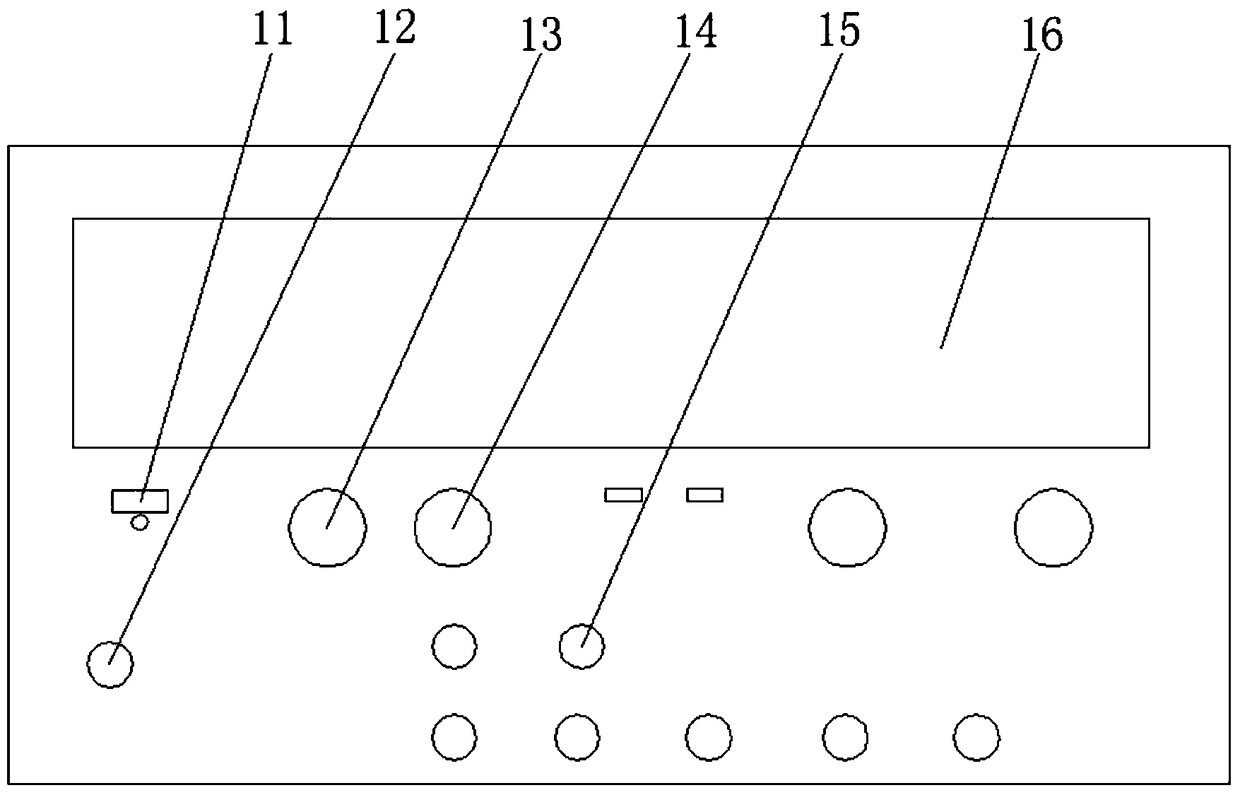

Image

  • Method and device for detecting blind hole of circuit board
  • Method and device for detecting blind hole of circuit board
  • Method and device for detecting blind hole of circuit board

Examples


Embodiment Construction

[0028] In order to make the purpose, technical solutions and advantages of the present invention clearer, the technical solutions in the embodiments of the present invention will be clearly and completely described below in conjunction with the accompanying drawings in the embodiments of the present invention. Obviously, the described embodiments are only Some, but not all, embodiments of the invention. Based on the embodiments of the present invention, all other embodiments obtained by persons of ordinary skill in the art without making creative efforts belong to the protection scope of the present invention.

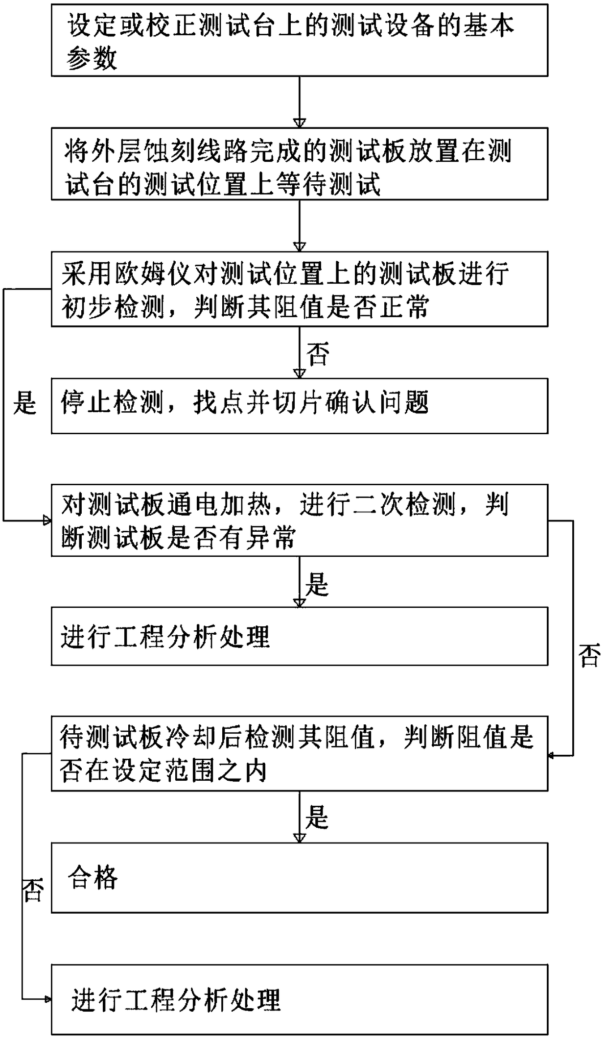
[0029] refer to figure 1 , figure 2 As shown, this embodiment provides a method for detecting blind holes on a circuit board, comprising the following steps:

[0030] S11 sets or corrects the basic parameters of the test equipment on the test bench; specifically, the test bench described in this embodiment is provided with test equipment and an ohm meter, and the te...


PUM


Abstract

The invention discloses a method for detecting a blind hole of a circuit board. The method comprises the steps of: setting or correcting basic parameters of a test device on a test bench; placing a test board which has completed an outer-layer etching line on a test position of the test bench for testing; performing a primary detection on the test board on the test position by an ohmmeter, and determining whether the resistance value is normal; if not, stopping the detection, finding a point and slicing to confirm the problem; if yes, electric heating the test board to perform a secondary detection, and determining whether the test board is abnormal; if yes, performing engineering analysis processing; if not, detecting the resistance value of the board to be tested after cooling, and determining whether the resistance value is within a set range; if yes, determining the board is qualified; if not, performing engineering analysis processing. The method uses the ohmmeter combined with high heat induced by high current going through a circuit to detect the resistance and the heat resistance of the blind hole of the circuit board, so that the abnormality can be timely discovered duringthe process control, and the scrap rate can be reduced from 0.5% to 0.05%.

Description

technical field [0001] The invention relates to the technical field of circuit board detection, in particular to a method for detecting blind holes in a circuit board and detection equipment thereof. Background technique [0002] In the electroplating process of printed circuit board (PCB), the copper plating layer is mainly divided into two types, one is the whole board copper plating, which prevents the electroless copper plating layer from being oxidized and corroded by acid through electroplating thickening. The other is pattern electroplating, which thickens the copper layer in the hole and the copper layer of the line or serves as the base of the nickel plating layer. With the large-scale development of portable electronic products, "high density" has become one of the important development trends of PCB, and directly promotes the development of micro-via technology closely related to this industry. [0003] Micro vias are mainly divided into three categories, namely:...

Claims


Application Information

Patent Timeline
Patent Type & Authority Applications(China)
IPC IPC(8): G01R31/28
CPCG01R31/2806
Inventor 刘艳华
Owner 昆山中哲电子有限公司
Learn More