Surface modification method of flexible stretchable circuit and application thereof
A surface modification and flexible technology, applied in photolithography/patterning, patterning and photolithography, pattern formation by transfer, etc., can solve problems such as damage, failure to provide sufficient biocompatibility, and failure to function normally
- Summary
- Abstract
- Description
- Claims
- Application Information
AI Technical Summary
Problems solved by technology
Method used
Image
Examples
Embodiment 1
[0085] This example is used to illustrate the flexible and stretchable conductive circuit prepared by the method of the present invention.
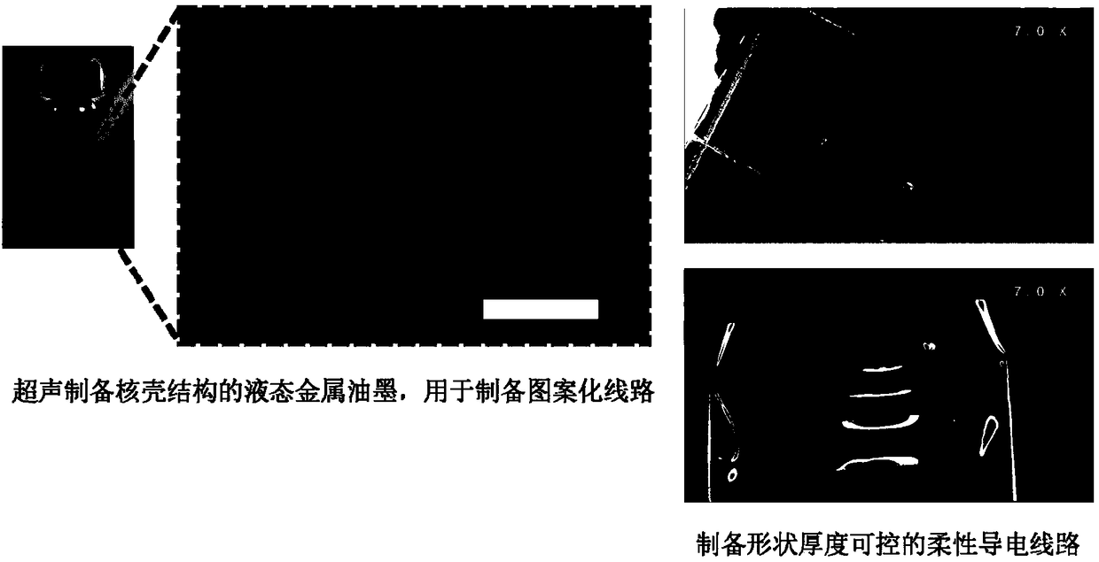
[0086] Put 1g of liquid indium gallium eutectic alloy (EGaIn Ga 75.5%wt In 24.5%wt) in 1ml of mixed solution of n-octanol and glycerol (volume ratio octanol: glycerol=80:20), use Ultrasonic cell disruptor ultrasonicated at 30% amplitude for 60s to obtain a gray liquid metal suspension. The metal was dispersed into numerous micro-nano sized particles with an average particle size of 1500nm. The core of the small particles is liquid metal, and the outside is covered by a thin oxide film. In order to achieve complete transfer, the PET film was selected as the original pattern layer, and the PDMS solution was prepared according to the ratio of PDMS prepolymer: curing agent mass ratio of 10:1. A line width of 500 μm was produced on PET film using screen printing technology ( Figure 5 ) electrode pattern, and its width was measured with a hi...
Embodiment 2
[0088]This example is used to illustrate the flexible and stretchable conductive circuit prepared by the method of the present invention.
[0089] Put 1g of liquid indium gallium eutectic alloy (EGaIn Ga 75.5%wt In 24.5%wt) in 1ml of mixed solution of n-octanol and glycerol (volume ratio octanol: glycerol=80:20), use Ultrasonic cell breaker ultrasonicated at 30% amplitude for 20 minutes to obtain a gray liquid metal suspension. The metal was dispersed into numerous micro-nano-sized small particles, and the average particle size of the small particles was 800nm. The core of the small particles is liquid metal, and the outside is covered by a thin oxide film. In order to achieve complete transfer, the PET film was selected as the original pattern layer, and the PDMS solution was prepared according to the ratio of PDMS prepolymer: curing agent mass ratio of 10:1. A line width of 200 μm was fabricated on PET film using screen printing technology ( Image 6 ) electrode pattern, a...
Embodiment 3
[0091] This example serves to illustrate the direct surface modification of flexible and stretchable conductive circuits using the method of the present invention.
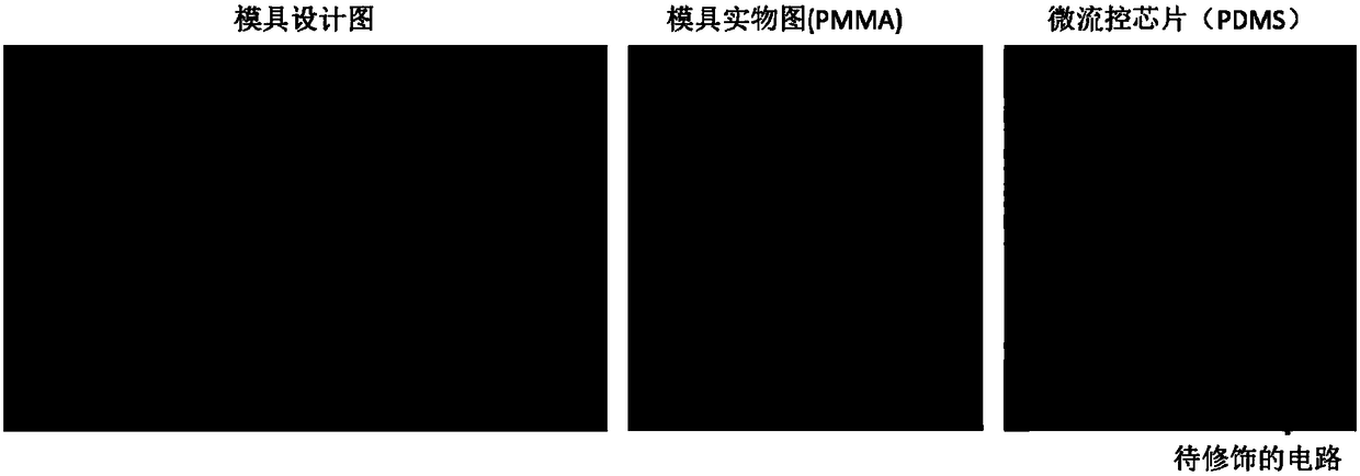
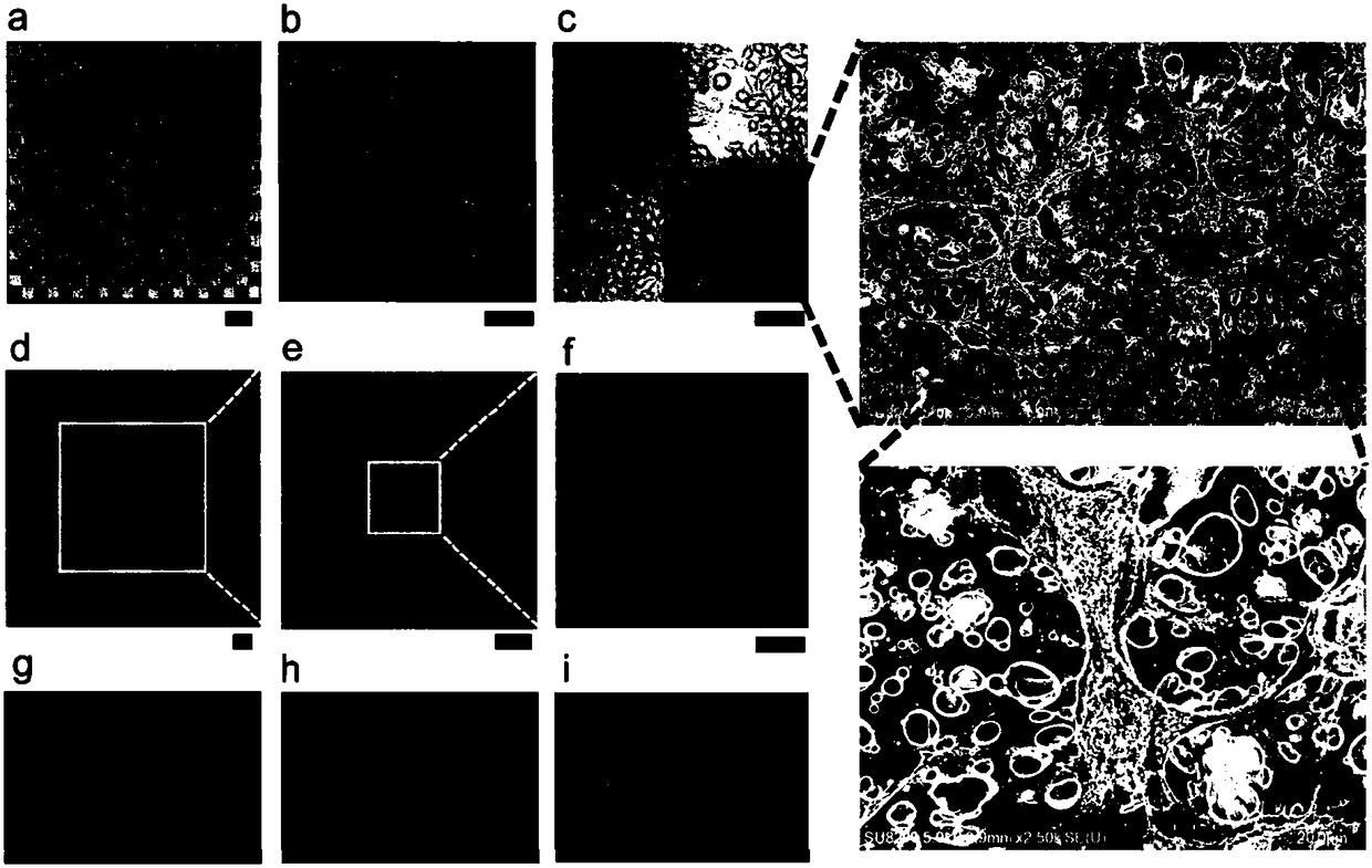
[0092] Using microfluidic technology, according to different circuit patterns, design microfluidic chips suitable for the shape of the circuit ( figure 2 ), add 1ml of Fibronectin solution with a concentration of 1mg / ml to the chip, cover the surface of the stretched line, incubate in the incubator at 37°C for 4 hours, take it out, and wash it gently once with PBS solution with a pH of 7.4. directly used to grow cells. The surface-modified stretched conductive circuit exhibits good biocompatibility, cells can adhere well to its surface, and maintain good activity after 7 days of culture ( image 3 ).
PUM
| Property | Measurement | Unit |
|---|---|---|
| The average particle size | aaaaa | aaaaa |
| The average particle size | aaaaa | aaaaa |
Abstract
Description
Claims
Application Information
 - R&D Engineer
- R&D Manager
- IP Professional
- Industry Leading Data Capabilities
- Powerful AI technology
- Patent DNA Extraction
Browse by: Latest US Patents, China's latest patents, Technical Efficacy Thesaurus, Application Domain, Technology Topic, Popular Technical Reports.
© 2024 PatSnap. All rights reserved.Legal|Privacy policy|Modern Slavery Act Transparency Statement|Sitemap|About US| Contact US: help@patsnap.com


