Nano-porous LED array chip with anti-reflection passivation layer and preparation method thereof

A technology of LED arrays and nanoholes, applied in electrical components, electrical solid devices, circuits, etc., can solve the disadvantages of high signal-to-noise ratio and high-speed visible light communication, large difference in refractive index between GaN material and air, and large thickness of electron injection layer and other issues, to achieve high yield, meet the isolation effect, and reduce the effect of leakage

Pending Publication Date: 2019-01-08
SOUTH CHINA UNIV OF TECH
View PDF0 Cites 6 Cited by
  • Summary
  • Abstract
  • Description
  • Claims
  • Application Information

AI Technical Summary

Problems solved by technology

However, the formation of photonic crystals requires strictly periodic distribution of nanostructures. GaN-based resonators require complex technologies such as laser stripping sapphire substrates or epitaxial distributed Bragg mirrors. Surface plasmons are limited by local field enhancement characteristics and space. The contradiction between the thickness of the hole / electron injection layer is relatively large, and the process difficulty of these technologies is relatively large
In addition, due to the large difference in refractive index between the GaN material and air, when the light exits from the inside of the LED chip, the light escape cone is small and the light extraction efficiency is low, which is not conducive to high signal-to-noise ratio and high-speed visible light communication.

Method used


Image

  • Nano-porous LED array chip with anti-reflection passivation layer and preparation method thereof
  • Nano-porous LED array chip with anti-reflection passivation layer and preparation method thereof
  • Nano-porous LED array chip with anti-reflection passivation layer and preparation method thereof

Examples


Embodiment 1

[0049] Embodiment 1, the preparation steps of the nanohole LED array chip with an anti-reflection passivation layer are as follows.

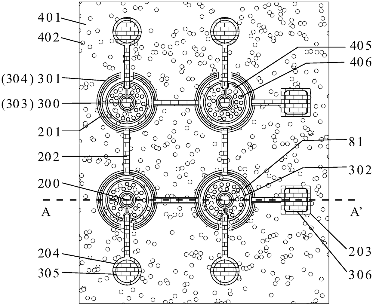
[0050] (1) GaN-based LED epitaxial wafers are prepared by metal oxide vapor deposition. The structure of GaN-based LED epitaxial wafers includes sapphire substrate 1, GaN buffer layer 2, unintentionally doped GaN layer 3, and N-type doped GaN layer. 4. Quantum well layer 5 , P-type doped AlGaN layer 6 and P-type doped GaN layer 7 . Such as Figure 3a shown.

[0051] (2) Deposit a transparent current spreading layer ITO 8 with a thickness of 100 nm on the GaN-based LED epitaxial wafer using electron beam evaporation, in N 2 200sccm, O 2 Rapid annealing in a mixed atmosphere of 35 sccm for 3 minutes to form an ohmic contact, and then use ultraviolet lithography and wet etching, and soak in ITO etching solution for 15 minutes at room temperature to form an ITO disk distributed only in the active area of ​​the light-emitting unit. The diameter ...


PUM

PropertyMeasurementUnit
Diameteraaaaaaaaaa
Depthaaaaaaaaaa
Widthaaaaaaaaaa

Abstract

The invention discloses a nano-hole LED array chip with an antireflection passivation layer and a preparation method thereof. The LED array chip of the invention is composed of N * N light emitting units, the anode of each light emitting unit is independently led out, and all light emitting units share a cathode; The active region of the luminescent cell has deep nanopores, and the depth of the nanopores exceeds the depth of the quantum well layer. The dielectric thin film layer on the surface of GaN material also has shallow nanopores, and the bottom of nanopores has dielectric thin film. Asthat dielectric passivation lay on the active region is slotted, Combined with soft film nanoimprinting technology, the deep nanopore and the shallow nanopore of the passivation layer can be preparedsimultaneously, the deep nanopore of the active region enhances the radiation recombination rate, and the shallow nanopore of the passivation layer constitutes an antireflective passivation layer, which is beneficial to the escape of photon mode, the light emission efficiency and the modulation bandwidth. In addition, the preparation method of the invention avoids the deep etching process, and hasthe advantages of simple process and high yield.

Description

technical field [0001] The invention relates to the field of LED chips, in particular to a micro-sized LED array chip with a nanohole structure for visible light communication and a preparation method thereof. Background technique [0002] Visible light communication is an important breakthrough point of LED (light-emitting diode) beyond the field of lighting. In order to increase the modulation bandwidth of the visible light communication system, the feedback circuit of the signal receiver can be optimized, or the frequency point with excessive loss can be raised by using an equalization circuit. This technology is low in cost and effective, but because the frequency point to be processed is not only closely related to the equivalent resistance and equivalent capacitance of the LED device, but also closely related to the parasitic resistance and parasitic capacitance of the entire system, the adjustment of the circuit is often only applicable Specific to specific LED devic...

Claims


Application Information

Patent Timeline
IPC IPC(8): H01L27/15H01L33/44H01L33/20H01L33/00
CPCH01L27/156H01L33/007H01L33/20H01L33/44
Inventor 黄华茂黄程吴浩城王洪
Owner SOUTH CHINA UNIV OF TECH
Why Eureka
Try Eureka