Deformation stress sensor based on strontium niobate titanate resistive thin film
A technology of doping strontium niobium titanate and deformation stress, which is applied in the field of microelectronics, can solve the problems of inability to realize flexible functions, high power consumption, and low sensitivity, and achieve the effects of good piezoresistive effect, improved performance, and high sensitivity
- Summary
- Abstract
- Description
- Claims
- Application Information
AI Technical Summary
Problems solved by technology
Method used
Image

Examples
Embodiment 1
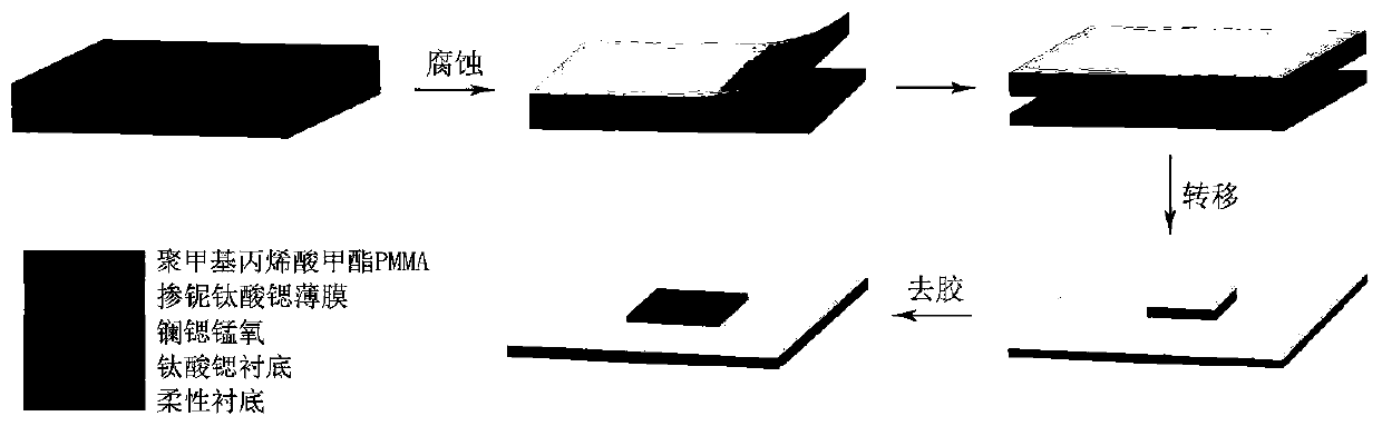
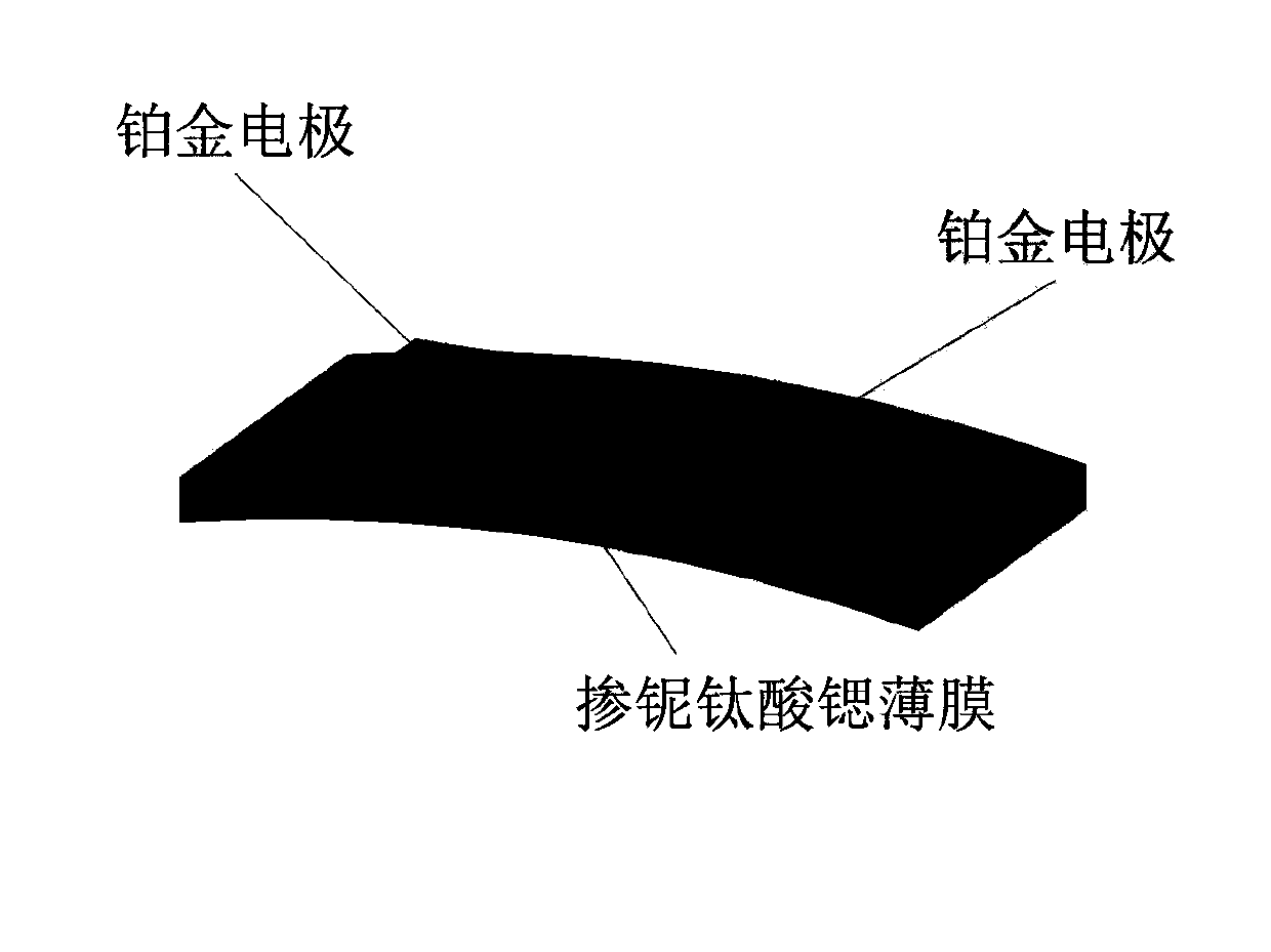
[0031] Embodiment 1: Fabricate a deformation stress sensor with a single-sided platinum-platinum electrode structure.
[0032] Step 1: growing a lanthanum strontium manganese oxide thin film on a strontium titanate substrate.
[0033] 1a) Put the strontium titanate substrate, the lanthanum strontium manganese oxide target, and the strontium niobate-doped strontium titanate target into the reaction chamber of the pulsed laser deposition system, and evacuate the reaction chamber until the vacuum degree reaches 1*10 -6 Below mbar;
[0034] 1b) Introduce oxygen into the reaction chamber to maintain the oxygen pressure in the reaction chamber at 0.1mbar, and set the energy density of the laser to 1.1J / cm 2 The sum frequency is 5Hz, the temperature of the substrate is set to 700°C, the laser emits laser light, and the lanthanum strontium manganese oxide target is burned 5000 times, so that the burnt out lanthanum strontium manganese oxide plasma is deposited on the strontium titana...
Embodiment 2
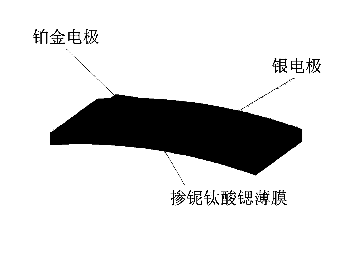
[0046] Embodiment 2: Fabricate a deformation stress sensor with a single-sided platinum-silver electrode structure.
[0047] Step 1: growing a lanthanum strontium manganese oxide thin film on a strontium titanate substrate.
[0048] The specific implementation of this step is the same as step 1 in Embodiment 1.
[0049] Step 2: depositing a layer of strontium niobate-doped titanate film on the lanthanum strontium manganese oxide film.
[0050] The specific implementation of this step is the same as step 2 in Embodiment 1.
[0051] Step 3: Spin-coat polymethyl methacrylate PMMA on the strontium niobate-doped titanate thin film.
[0052] The specific implementation of this step is the same as step 3 in Embodiment 1.
[0053] Step 4: separating the strontium niobate titanate film attached with polymethyl methacrylate PMMA from the substrate.
[0054] The specific implementation of this step is the same as step 4 in Embodiment 1.
[0055] Step 5: Obtain a high-quality self-su...
Embodiment 3
[0058] Embodiment 3: Manufacturing a deformation stress sensor with a double-sided platinum-platinum electrode structure.
[0059] Step A: growing a lanthanum strontium manganese oxide film on a strontium titanate substrate.
[0060] The specific implementation of this step is the same as step 1 in Embodiment 1.
[0061] Step B: Depositing a layer of strontium niobate-doped titanate film on the lanthanum strontium manganese oxide film.
[0062] The specific implementation of this step is the same as step 2 in Embodiment 1.
[0063] Step C: Spin-coat polymethyl methacrylate PMMA on the strontium niobate-doped titanate thin film.
[0064] The specific implementation of this step is the same as step 3 in Embodiment 1.
[0065] Step D: separating the strontium niobate titanate thin film attached with polymethyl methacrylate PMMA from the substrate.
[0066] The specific implementation of this step is the same as step 4 in Embodiment 1.
[0067] Step E: High-quality self-suppo...
PUM
| Property | Measurement | Unit |
|---|---|---|
| thickness | aaaaa | aaaaa |
Abstract
Description
Claims
Application Information
 - Generate Ideas
- Intellectual Property
- Life Sciences
- Materials
- Tech Scout
- Unparalleled Data Quality
- Higher Quality Content
- 60% Fewer Hallucinations
Browse by: Latest US Patents, China's latest patents, Technical Efficacy Thesaurus, Application Domain, Technology Topic, Popular Technical Reports.
© 2025 PatSnap. All rights reserved.Legal|Privacy policy|Modern Slavery Act Transparency Statement|Sitemap|About US| Contact US: help@patsnap.com