
Ohmic contact structure of nitride semiconductor device and manufacturing method thereof

A nitride semiconductor and ohmic contact technology, which is applied in semiconductor/solid-state device manufacturing, semiconductor devices, electrical components, etc., can solve problems such as the lateral diffusion of aluminum elements, achieve reduced interface states, good effects, and improve the lateral diffusion of aluminum elements. Effect

Inactive Publication Date: 2018-08-24
XIAMEN SANAN INTEGRATED CIRCUIT
View PDF10 Cites 1 Cited by
  • Summary
  • Abstract
  • Description
  • Claims
  • Application Information

AI Technical Summary

Problems solved by technology

[0005] The main purpose of the present invention is to provide a method for preventing lateral diffusion of ohmic metal aluminum elements in GaN-based devices, so as to solve the problem of lateral diffusion of aluminum elements in GaN-based device ohmic metal superalloys

Method used


Image

  • Ohmic contact structure of nitride semiconductor device and manufacturing method thereof
  • Ohmic contact structure of nitride semiconductor device and manufacturing method thereof

Examples


Embodiment Construction

[0024] The present invention will be described in further detail below in conjunction with the accompanying drawings and embodiments. The drawings of the present invention are only schematic diagrams for easier understanding of the present invention, and their specific proportions can be adjusted according to design requirements. Those skilled in the art should understand that the upper and lower relationships of relative components in the figures described herein refer to the relative positions of the components, so all of them can be turned over to present the same components, which should all fall within the scope of the present specification.

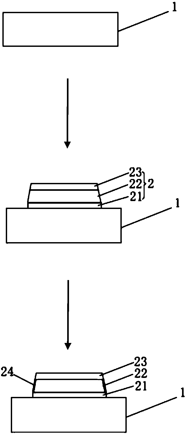
[0025] refer to figure 1 , a method for manufacturing an ohmic contact of a nitride semiconductor device is realized by the following steps:

[0026] A metal stack structure 2 is formed on the GaN substrate 1 , and the metal stack structure 2 includes a diffusion barrier layer 21 , an Al layer 22 and an upper metal layer 23 deposit...


PUM

PropertyMeasurementUnit
thicknessaaaaaaaaaa
thicknessaaaaaaaaaa

Abstract

The present invention discloses a manufacturing method of an Ohmic contact structure of a nitride semiconductor device. The method comprises the steps of: forming a metal stacked structure including an Al layer on a GaN substrate, performing low-temperature oxidation in an oxygen atmosphere to form an aluminum oxide barrier layer at the side wall of the Al layer, and forming Ohmic contact of the metal stacked structure and the GaN substrate through high-temperature alloy. The low-temperature oxidation processing is performed prior to Ohmic contact alloy to allow the outer side of the Ohmic metal to be oxidized to aluminum oxide so as to reduce the interface pollution or improve an interface state; and moreover, the method increases low-temperature oxidation in a traditional GaN device Ohmic metal manufacturing process, is simple in process with no need for introducing other substances and other materials, and is high in practicability and good in effect.

Description

technical field [0001] The invention relates to a semiconductor manufacturing process, in particular to an ohmic contact structure of a nitride semiconductor device and a manufacturing method thereof. Background technique [0002] The third-generation semiconductor material GaN has a large band gap (3.4eV), high electron saturation rate (2×10 7 cm / s), high breakdown electric field (1×10 10 ~3×10 10 V / cm), high thermal conductivity, corrosion resistance and radiation resistance have become current research hotspots and have broad application prospects. In particular, AlGaN / GaN heterojunction HEMTs (High electronmobility transistors) have the advantages of high frequency, high power density and high operating temperature, and are the development direction of solid-state microwave power devices and power electronic devices. [0003] The ohmic contact process is one of the key technologies for making high-performance GaN-based devices, which directly affects the performance o...

Claims


Application Information

Patent Timeline
Patent Type & Authority Applications(China)
IPC IPC(8): H01L21/24H01L21/283H01L29/45
CPCH01L29/45H01L21/244H01L21/283H01L29/2003H01L29/401H01L29/452H01L21/28575H01L21/246
Inventor 刘胜厚林光耀周泽阳许若华蔡文必
Owner XIAMEN SANAN INTEGRATED CIRCUIT
Learn More