Fabrication method of P-type crystal-silicon solar cell with passivation back surface

A solar cell, backside passivation technology, applied in circuits, photovoltaic power generation, electrical components, etc., can solve the problems of reduced minority carrier lifetime, mechanical damage of passivation layer, increased resistance of ohmic contact between electrodes and silicon wafers, etc., to optimize the emitter. , Improve the power supply voltage, improve the effect of photoelectric conversion efficiency

Inactive Publication Date: 2018-07-27
南通苏民新能源科技有限公司
View PDF6 Cites 5 Cited by
  • Summary
  • Abstract
  • Description
  • Claims
  • Application Information

AI Technical Summary

Problems solved by technology

Since the electrode should be fully in contact with the silicon wafer, it is necessary to perform laser grooving on the oxide film on the surface of the silicon wafer in the area where the electrode passes. However, since the laser is a light source with high energy and high heat, the surface of the silicon wafer will A layer of oxide film will be formed, which increases the ohmic contact between the electrode and the silicon wafer. At the same time, the laser will also cause certain mechanical damage to the passivation layer, and generate new recombination centers, resulting in a decrease in the minority carrier lifetime.

Method used


Image

  • Fabrication method of P-type crystal-silicon solar cell with passivation back surface
  • Fabrication method of P-type crystal-silicon solar cell with passivation back surface
  • Fabrication method of P-type crystal-silicon solar cell with passivation back surface

Examples


Embodiment Construction

[0030] In order to make the object, technical solution and advantages of the present invention more clear, the present invention will be further described in detail below in conjunction with the examples. It should be understood that the specific embodiments described here are only used to explain the present invention, not to limit the present invention.

[0031] The application principle of the present invention will be described in detail below in conjunction with the accompanying drawings.

[0032] In the present invention, the used crystalline silicon chip for making the battery is a P-type crystalline silicon chip containing B. For the sake of distinction, the front side of the silicon chip described below is the side where the PN junction is formed on the surface, and the back side of the silicon chip is the opposite side of the front.

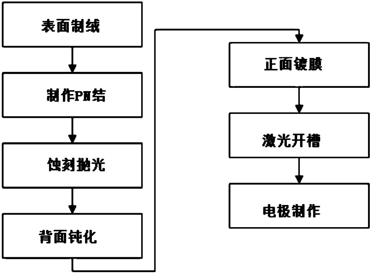
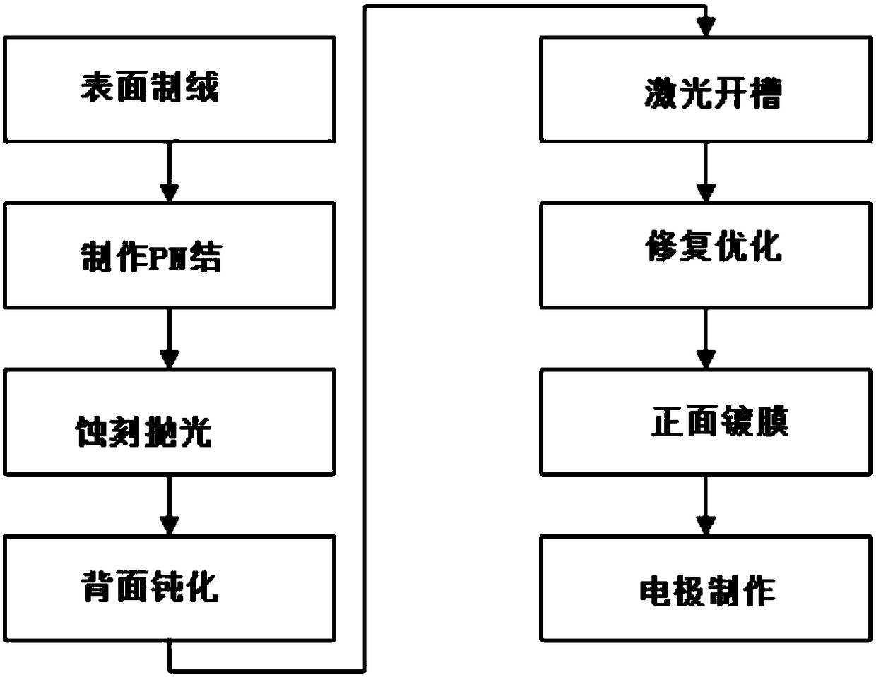
[0033] Such as figure 2 The manufacturing process flow chart of the P-type crystalline silicon solar cell with passivation on the ba...


PUM


Abstract

The invention discloses a fabrication method of a P-type crystal-silicon solar cell with a passivation back surface. Planarization recovery processing is performed on a bottom surface and a side wallof a laser groove in a back surface of a silicon wafer by a chemical etching method with regard to the silicon wafer after being grooved by laser, a diffusion layer on a front surface of the silicon wafer is simultaneously etched, the concentration gradient of doping phosphate atoms in the diffusion layer is optimized, an emitter is optimized, and a SiO2 thin film and a second silicon nitride anti-reflection film are deposited on the front surface of the silicon wafer. According to the fabrication method, the open-circuit voltage and the photovoltaic conversion efficiency of a solar cell pieceare improved by recovering a damage layer.

Description

technical field [0001] The invention belongs to the field of solar photovoltaic cell manufacturing, and in particular relates to a method for manufacturing a P-type crystalline silicon solar cell with passivation on the back. Background technique [0002] During the manufacturing process of solar cells, the lattice defects on the surface of the silicon wafer will reduce the photoelectric conversion efficiency of the solar cell, so a back passivation technology is used to deposit a dense oxide film on the surface of the cell to reduce the surface of the silicon wafer. compound center. Since the electrode should be fully in contact with the silicon wafer, it is necessary to perform laser grooving on the oxide film on the surface of the silicon wafer in the area where the electrode passes. However, since the laser is a light source with high energy and high heat, the surface of the silicon wafer will A layer of oxide film will be formed, which increases the ohmic contact betwe...

Claims


Application Information

Patent Timeline
Patent Type & Authority Applications(China)
IPC IPC(8): H01L31/0352H01L31/068H01L31/18
CPCH01L31/035272H01L31/035281H01L31/068H01L31/1804Y02E10/547Y02P70/50
Inventor 徐华浦沈晶王玉涛张满良
Owner 南通苏民新能源科技有限公司
Why Eureka
Try Eureka