Nitride semiconductor structure and semiconductor light emitting element

A technology of nitride semiconductors and semiconductors, which is applied in the direction of semiconductor devices, electrical components, circuits, etc., can solve the problems of reducing the luminous efficiency of light-emitting diodes, affecting the luminous efficiency of light-emitting diodes, and deteriorating interface characteristics, so as to increase internal quantum efficiency and improve internal Quantum efficiency, the effect of reducing compressive stress

Inactive Publication Date: 2018-07-20
GENESIS PHOTONICS INC
View PDF7 Cites 3 Cited by
  • Summary
  • Abstract
  • Description
  • Claims
  • Application Information

AI Technical Summary

Problems solved by technology

[0006] The method of using p-AlGaN as a p-type carrier blocking layer can effectively confine carriers in the quantum well layer to improve the internal quantum efficiency of light-emitting diodes; however, since the multiple quantum well structure is generally based on the quantum well layer and GaN quantum barrier layer, and in essence, the p-AlGaN p-type carrier barrier layer and GaN quantum barrier layer have a very high lattice mismatch, making the InGaN quantum well layer due to lattice The mismatch will be severely affected by the compressive stress, and this compressive stress changes the energy band structure of each quantum well layer, so that the electrons and holes in the quantum well layer are separated from each other in space, resulting in the light-emitting diode. The luminous efficiency is reduced; moreover, the above-mentioned compressive stress will also deteriorate the interface characteristics between the adjacent GaN quantum barrier layer and the InGaN quantum well layer, thereby losing carriers at the interface, and also affecting the luminous efficiency of the light-emitting diode

Method used


Image

  • Nitride semiconductor structure and semiconductor light emitting element
  • Nitride semiconductor structure and semiconductor light emitting element

Examples


Embodiment Construction

[0046] The purpose of the present invention and its structural design and functional advantages will be described according to the following drawings and preferred embodiments, so as to have a more in-depth and specific understanding of the present invention.

[0047] First of all, in the description of the following embodiments, it should be understood that when it is indicated that a layer (or film) or a structure is disposed "on" or "under" another substrate, another layer (or film), or another structure , which can be "directly" located on other substrates, layers (or films), or another structure, or have more than one intermediate layer between them in an "indirect" manner. The location of each layer can be described with reference to the drawings.

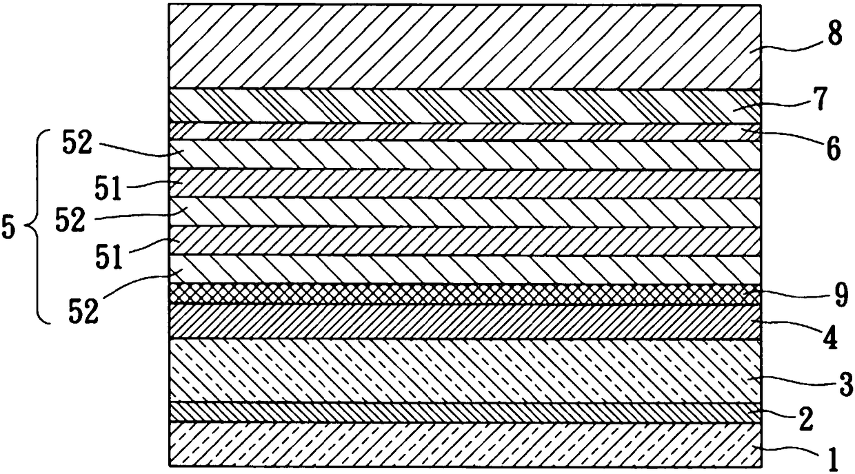
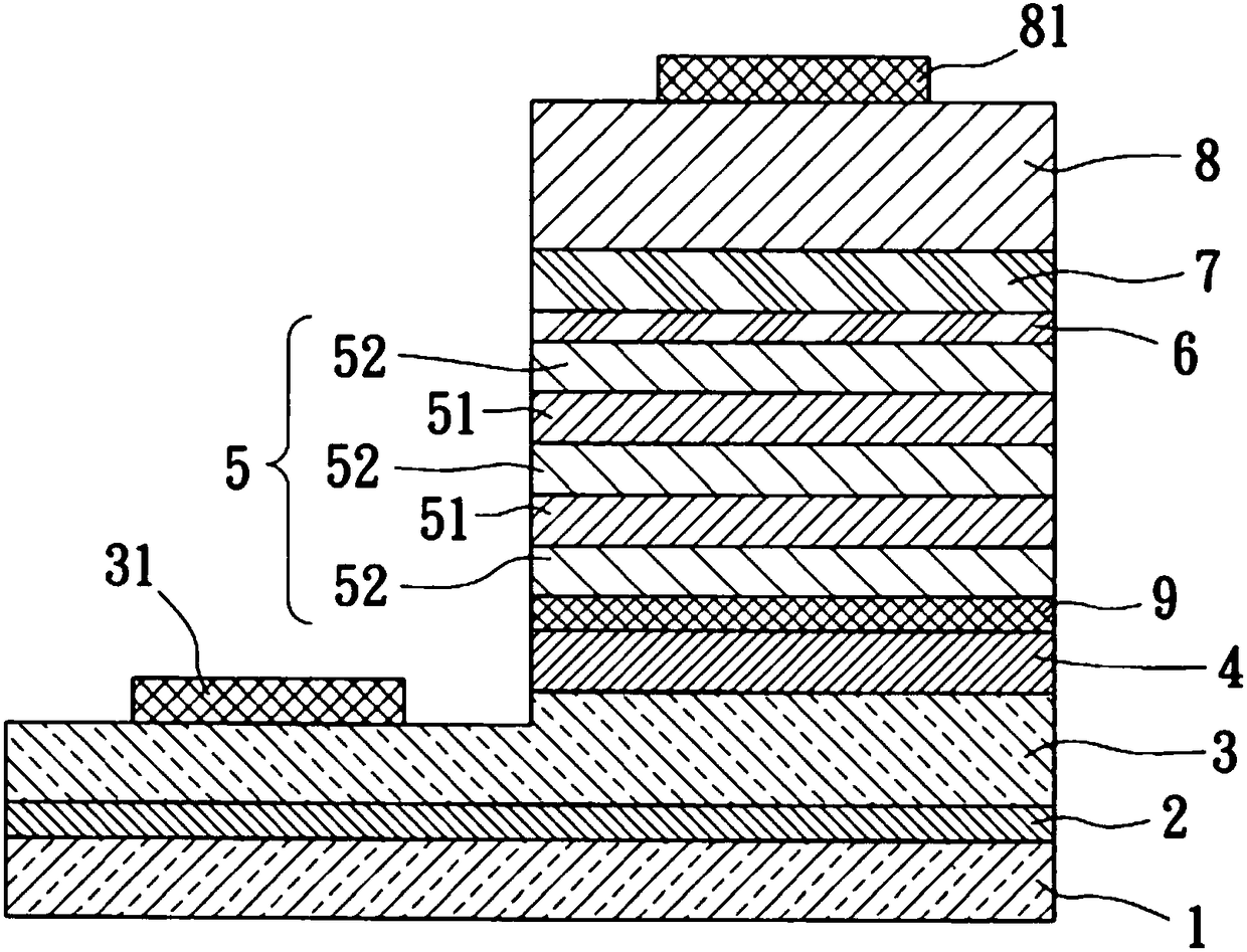
[0048] see figure 1 As shown, it is a schematic cross-sectional view of a nitride semiconductor structure provided by a preferred embodiment of the present invention. It is mainly configured with a stress control layer 6 betw...


PUM


Abstract

The invention discloses a nitride semiconductor structure and a semiconductor light emitting element. According to the nitride semiconductor structure, a stress control layer is mainly configured between a light emitting layer and a p type carrier block layer; the p type carrier block layer is formed by a material shown as Al<x>Ga<1-x>N 0<x<1; the stress control layer is formed by a material shownas Al<x>In<y>Ga<1-x-y>N 0<x<1, 0<y<1, 0<(x+y)<1; the light emitting layer has multiple well layers which are alternately stacked, and a multi-quantum-well structure of block layers; and one well layer is formed between every two block layers. The semiconductor light emitting element at least comprises the nitride semiconductor structure, and an n type electrode and a p type electrode which are intwo-phase matching for providing electric energy. Therefore, the stress control layer not only can relieve the problem of crystal quality degradation caused by lattice mismatch between the p type carrier block layer and the light emitting layer, but also can lower compression stress caused by material difference of the well layers.

Description

[0001] The present invention is a divisional application of the invention patent application with the application number 201310029711.7 and the invention name "Nitride Semiconductor Structure and Semiconductor Light-Emitting Element" filed on January 25, 2013. technical field [0002] The present invention relates to a nitride semiconductor structure and a semiconductor light-emitting element, in particular to a kind of aluminum alloy arranged between the light-emitting layer and the p-type carrier blocking layer. x In y Ga 1-x-y The invention relates to a nitride semiconductor structure and a semiconductor light-emitting element of a stress control layer composed of N materials, belonging to the field of semiconductor technology. Background technique [0003] In recent years, the application of light-emitting diodes has become more and more extensive, and has become an indispensable and important component in daily life; and light-emitting diodes are expected to replace to...

Claims


Application Information

Patent Timeline
Patent Type & Authority Applications(China)
IPC IPC(8): H01L33/12H01L33/06H01L33/32
CPCH01L33/06H01L33/12H01L33/32
Inventor 黄吉丰林京亮王信介吴俊德李玉柱李俊杰
Owner GENESIS PHOTONICS INC
Why Eureka
Try Eureka