Method for forming film
一种成膜方法、氧化膜的技术,应用在电气元件、半导体/固态器件制造、电路等方向,达到抑制SiC形成、高生产能力、界面平坦的效果
- Summary
- Abstract
- Description
- Claims
- Application Information
AI Technical Summary
Problems solved by technology
Method used
Image

Examples
Embodiment
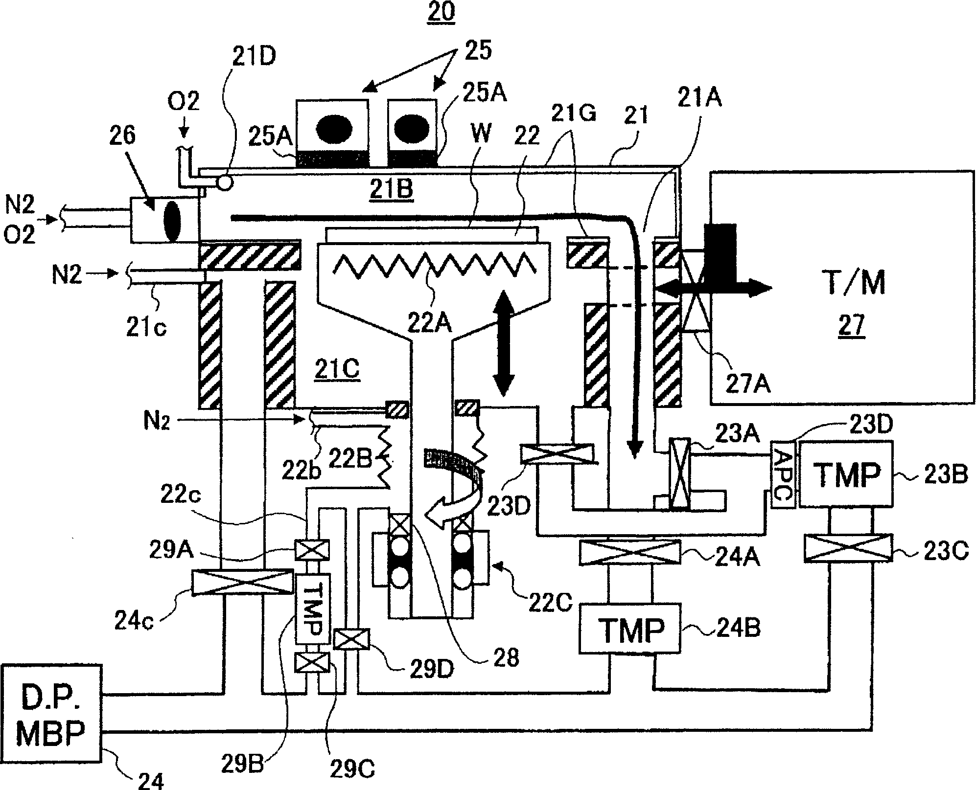
[0121] Thus, by using figure 1 The substrate processing apparatus 20 can form a high-quality silicon oxide film, silicon nitride film, or silicon oxynitride film on the surface of a silicon substrate at a low temperature below 450° C. Perform the above UV-O at high substrate temperature 2 processing or above RF-N 2 Treatment to obtain higher quality silicon oxide film or nitride film expectations.
[0122]Preferred embodiments of the present invention corresponding to such desires are described below.
no. 1 example
[0124] Figure 7 shows the flow of the film formation process in the first embodiment of the present invention picture .
[0125] refer to Figure 7 , in this embodiment, in step 11, the silicon substrate is introduced into figure 1 In the processing container 21 of the substrate processing device 20; in step 12, the substrate is heated to a processing temperature above 450°C, such as about 650-750°C; in step 13, the above-mentioned UV-O is carried out at the above-mentioned processing temperature 2 treatment to form a high-quality silicon oxide film (radical oxide film) on the surface of the above-mentioned silicon substrate. Furthermore, if necessary, in step 14, by performing RF-N 2 treatment to convert the aforementioned silicon oxide film into an oxynitride film.
[0126] as Figure 7 The heating process 12, Figure 8 Indicates one of the heating schemes currently in use.
[0127] refer to Figure 8 A silicon substrate with a diameter of 30 cm and a clean surfac...
no. 2 example
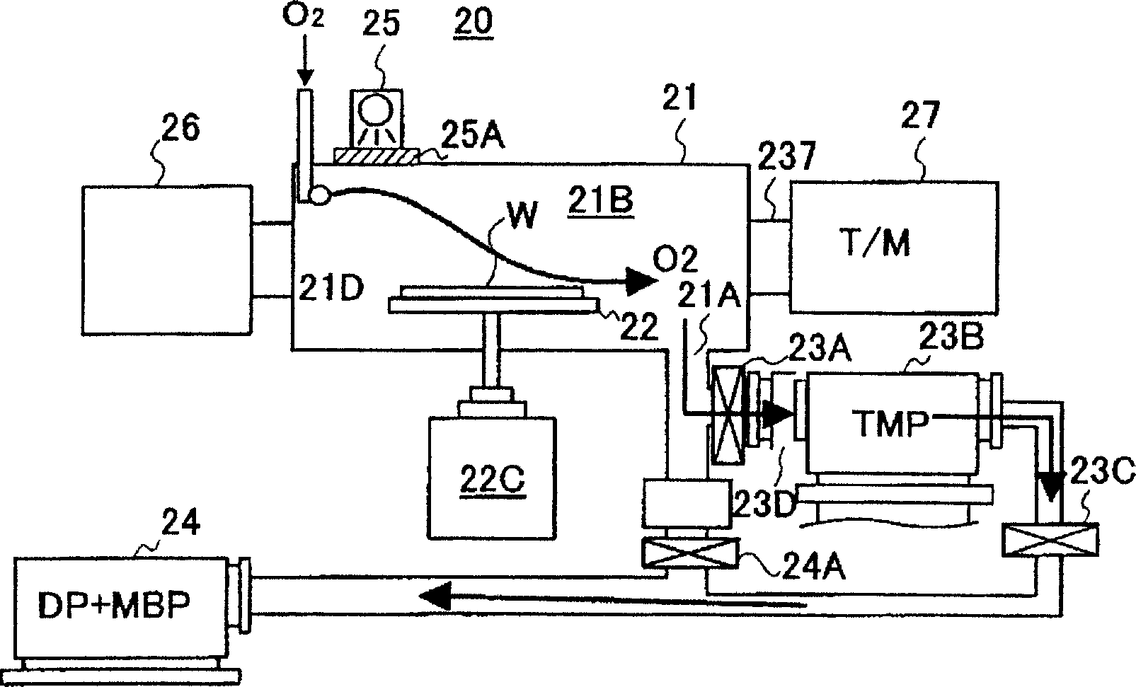
[0194] Figure 24 A film forming method according to a second embodiment of the present invention is shown.
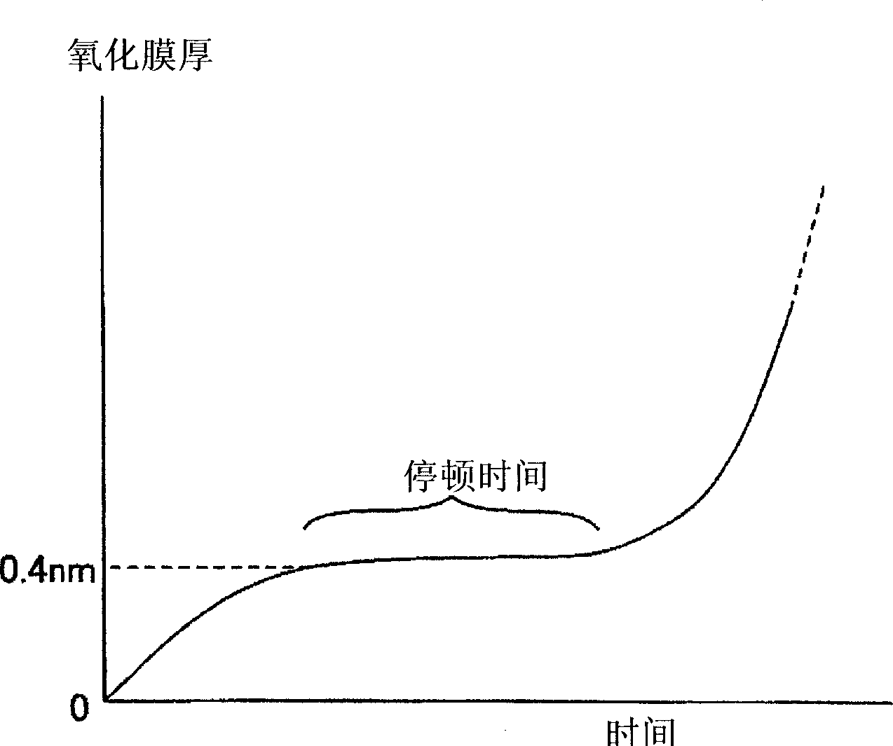
[0195] refer to Figure 24 , in this embodiment, in step 1, the silicon substrate cleaned by DHF is introduced into the processing container 21 of the above-mentioned substrate processing device 20 as the above-mentioned processing substrate W; in step 2, in N 2 or in an inert atmosphere such as Ar, the temperature of the above-mentioned silicon substrate is raised to a temperature of 450°C where SiC will not be formed; then, in step 3, the above-mentioned UV-O 2 treatment to form a uniform silicon oxide film of about 0.4 nm on the surface of the silicon substrate. When the substrate temperature is set below 450°C, the hydrogen atoms terminated on the surface of the silicon substrate are not detached, and the surface of the silicon substrate is terminated by hydrogen. 2 Oxidation, so SiC will not form on the substrate surface.
[0196] exist Figure 24 In the film...
PUM
| Property | Measurement | Unit |
|---|---|---|
| wavelength | aaaaa | aaaaa |
| diameter | aaaaa | aaaaa |
| diameter | aaaaa | aaaaa |
Abstract
Description
Claims
Application Information
 - R&D
- Intellectual Property
- Life Sciences
- Materials
- Tech Scout
- Unparalleled Data Quality
- Higher Quality Content
- 60% Fewer Hallucinations
Browse by: Latest US Patents, China's latest patents, Technical Efficacy Thesaurus, Application Domain, Technology Topic, Popular Technical Reports.
© 2025 PatSnap. All rights reserved.Legal|Privacy policy|Modern Slavery Act Transparency Statement|Sitemap|About US| Contact US: help@patsnap.com