Flash memory manufacturing method

A manufacturing method and technology of flash memory, which is applied in the field of flash memory manufacturing, can solve the problems affecting the programming and writing of memory cells, programming and writing function errors, etc., and achieve the effects of long annealing time, reducing leakage current, improving yield rate and electrical performance

Inactive Publication Date: 2018-02-02
SHANGHAI HUAHONG GRACE SEMICON MFG CORP
View PDF4 Cites 0 Cited by
  • Summary
  • Abstract
  • Description
  • Claims
  • Application Information

AI Technical Summary

Problems solved by technology

With the reduction of the critical size of the flash memory element storage unit, the number of electrons that can be captured by the floating gate in the flash memory element storage unit decreases. Less, in severe cases, it may change the written high level (more electrons) to low level (less electrons), which will affect the programming and writing of memory cells, resulting in errors in programming and writing functions

Method used


Image

  • Flash memory manufacturing method
  • Flash memory manufacturing method
  • Flash memory manufacturing method

Examples


Embodiment Construction

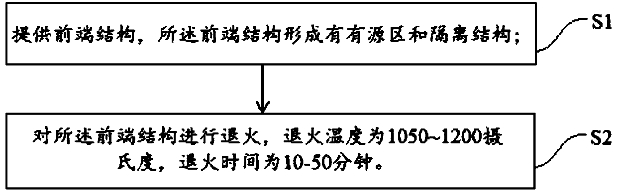
[0029] The specific implementation manner of the present invention will be described in more detail below with reference to schematic diagrams. Advantages and features of the present invention will be apparent from the following description and claims. It should be noted that all the drawings are in a very simplified form and use imprecise scales, and are only used to facilitate and clearly assist the purpose of illustrating the embodiments of the present invention.

[0030] The inventors have found that: figure 2 As shown, it is the flash memory structure in one embodiment of the present invention. When using the existing shallow trench isolation process to etch the trenches 12 to isolate multiple active regions 11, the incident ions with high energy and high density are more or less The ground will enter the active area 11. The high-energy incident ions will collide with the atoms on the lattice of the active region 11, causing some lattice atoms to be displaced, making t...


PUM


Abstract

The invention discloses a flash memory manufacturing method, which comprises the steps of providing a front-end structure, wherein the front-end structure is provided with an active region and an isolation structure; and performing annealing on the front-end structure, wherein the annealing temperature is 1050-1200 DEG C, and the annealing time is 10-50 minutes. According to the invention, annealing processing is performed on the front-end structure which is provided with the active region and the isolation structure, and the stress generated by crystal lattice deformation of the active regioncaused by groove etching or filling in the process of forming the isolation structure is released. Meanwhile, the split level of crystal lattices is reduced, crystal lattice defects of the active region are repaired, leakage current caused by the crystal lattice defects of the active region is reduced, and the electrical performance and the product yield of a flash memory are improved.

Description

technical field [0001] The invention relates to the technical field of semiconductor manufacturing, in particular to a flash memory manufacturing method. Background technique [0002] A flash memory element (Flash Memory, referred to as Flash) is a non-volatile memory element, which belongs to a type of memory device, and it can be used as a cache or as an underlying device for direct storage. Since data can be stored, read and erased multiple times, and the stored data will not disappear after power failure, it has been widely used in personal computers and other electronic devices. [0003] According to different logical structures, flash memory components can be mainly divided into NAND and NOR types. The former can provide larger capacity, but does not support local code execution, and the reading speed is slower (but the writing speed is faster); while NOR Small flash memory supports code running locally, and the read speed is slightly faster (and the write speed is sl...

Claims


Application Information

Patent Timeline
Patent Type & Authority Applications(China)
IPC IPC(8): H01L27/11521H01L21/324
CPCH01L21/324H10B41/30
Inventor 王鹏刘宇
Owner SHANGHAI HUAHONG GRACE SEMICON MFG CORP
Why Eureka
Try Eureka