Wafer-grade fan-out packaging structure and method

A technology of packaging structure and packaging method, applied in electrical components, electrical solid devices, circuits, etc., can solve the problems of poor electromagnetic shielding function and poor electrical performance of wafer-level packaging structure, so as to reduce impact and chip displacement. possibility, the effect of changing the flow trajectory

Active Publication Date: 2017-12-15
NAT CENT FOR ADVANCED PACKAGING
View PDF8 Cites 9 Cited by
  • Summary
  • Abstract
  • Description
  • Claims
  • Application Information

AI Technical Summary

Problems solved by technology

[0005] Therefore, the technical problem to be solved by the present invention is to solve the poor electromagnetic shielding function of the wafer-level packaging structure, the chip inside the packaging structure may be interfered by the electromagnetic wave interference of the packaging structure itself and the packaging structure, and the electrical performance of the wafer-level packaging structure. poor problem

Method used


Image

  • Wafer-grade fan-out packaging structure and method
  • Wafer-grade fan-out packaging structure and method
  • Wafer-grade fan-out packaging structure and method

Examples


Embodiment 1

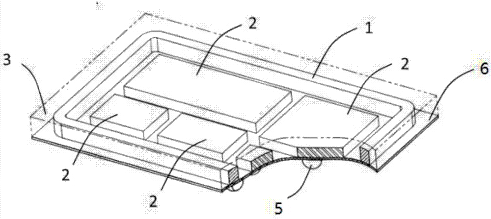
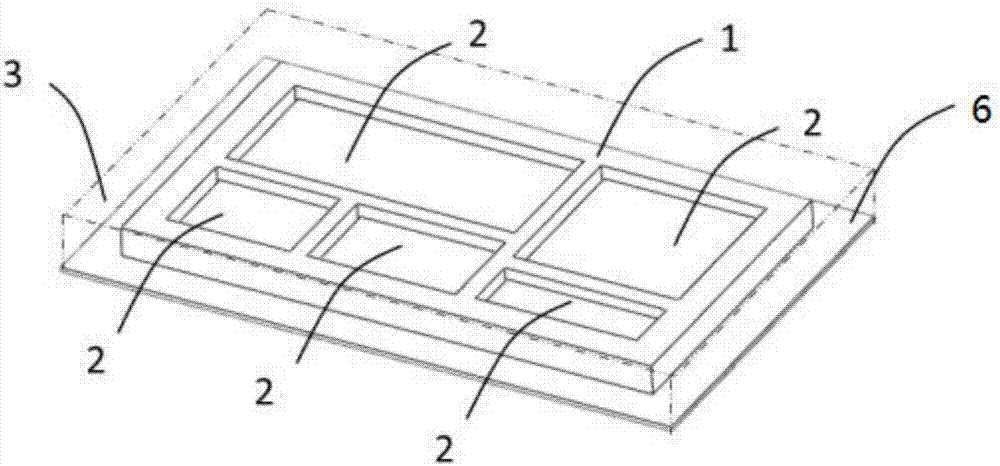
[0040] The embodiment of the present invention discloses a wafer-level fan-out packaging structure, please refer to figure 1 , figure 1 It is a schematic diagram of a three-dimensional structure of a wafer-level fan-out packaging structure disclosed in an embodiment of the present invention, including: a frame 1, which is used to place one or more chips 2; the frame 1 is connected to the ground; the package body 3. The frame 1 and the chip 2 are packaged in the package 3; the lower surface of the package 3 is located on the same plane as the lower surface of the frame 1 and the device surface of the chip 2. In this embodiment, the coefficient of linear expansion of the frame 1 is greater than that of the chip 2, and the frame 1 is a high-rigidity frame. Specifically, the material of the frame 1 is a metal conductor, such as copper, aluminum, alloy, etc. or the surface is plated with Metallic ceramic materials. Ground the metal or the metal-plated frame 1 so that the package ...

Embodiment 2

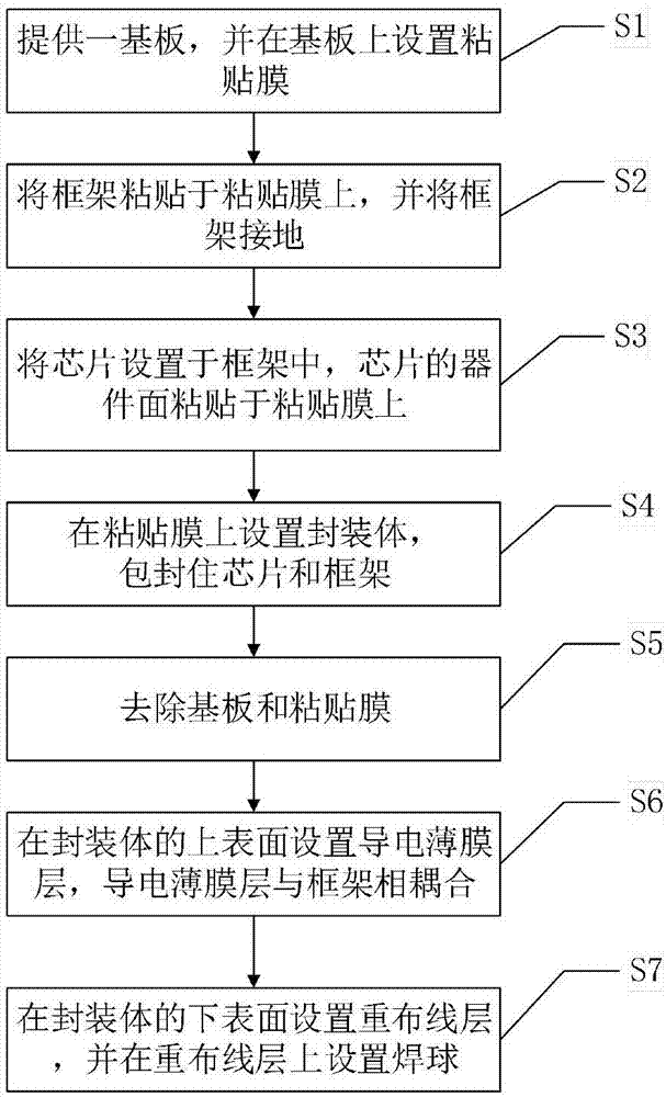
[0052] The embodiment of the present invention discloses a wafer-level fan-out packaging method, please refer to image 3 , image 3 A process flow chart of a wafer-level fan-out packaging method disclosed in this embodiment includes the following steps:

[0053] Step S1: providing a substrate, and setting an adhesive film on the substrate. Please refer to Figure 4 , Figure 4 It is a schematic diagram of setting an adhesive film on a substrate disclosed in an embodiment of the present invention. In this embodiment, the material of the substrate 7 can be a metal substrate or a glass substrate, and the adhesive film 8 can be a heat-peelable adhesive or a UV adhesive film. In a specific embodiment, the adhesive film 8 may be disposed on the substrate 7 by means of spray coating, spin coating, or film sticking. Preferably, the thickness of the adhesive film 8 is less than 100 um.

[0054] Step S2: Paste the frame on the adhesive film, and ground the frame. Please refer to ...


PUM


Abstract

The present invention discloses a structure and method of wafer-grade fan-out packaging with electromagnetic shielding. The structure comprises: a frame which is internally provided with one or more than one chips, wherein the frame is connected with a ground wire; a packaging body, wherein the frame and the one or more than one chips are packaged in the packaging body, and the lower surface of the packaging body, the lower surface of the frame and the devices of the one or more than one chips are located at the same plane. A metal conductor and the frame made of ceramic material and having a surface plated with metal are earthed to allow the packaging body and the frame in the wafer-grade fan-out packaging structure to form a complete loop so as to reduce the possibility of electromagnetic wave interference of the packaging structure itself and the external portion of the packaging structure on the wafer-grade packaging and the one or more than one chips at the internal portion of the structure and improve the electrical properties of the wafer-grade fan-out packaging structure.

Description

technical field [0001] The invention relates to the technical field of semiconductor packaging, in particular to a wafer-level fan-out packaging structure and a packaging method with an electromagnetic shielding function. Background technique [0002] With the increasing integration of electronic devices, the market is increasingly demanding microelectronic products with small size, high density and thin packaging. In order to adapt to the rapid increase in pin density per unit area of ​​the chip, wafer-level packaging technology has achieved a high degree of miniaturization. At the same time, with the reduction of chip size and the increase of wafer area, the manufacturing cost has been significantly reduced. Fan-out packaging technology is a branch of wafer-level packaging technology. Its package height and package size are greatly reduced. At the same time, its heat dissipation capability and signal integrity performance are good, and electromagnetic shielding can be dire...

Claims


Application Information

Patent Timeline
Patent Type & Authority Applications(China)
IPC IPC(8): H01L23/31H01L23/544H01L23/552H01L21/56
CPCH01L23/544H01L23/552H01L21/56H01L23/31H01L2224/12105H01L2224/96H01L2924/3025
Inventor 姚大平宋涛
Owner NAT CENT FOR ADVANCED PACKAGING
Why Eureka
Try Eureka