A kind of p-type diamond high and low potential barrier Schottky diode and its preparation method
A technology of Schottky diodes and diamonds, applied in the direction of diodes, semiconductor/solid-state device manufacturing, semiconductor devices, etc., can solve the contradictions of different heights, forward turn-on voltage and forward current density, and reverse leakage current and breakdown voltage and other problems, to achieve the effect of high current density, high breakdown voltage and small reverse leakage current
- Summary
- Abstract
- Description
- Claims
- Application Information
AI Technical Summary
Problems solved by technology
Method used
Image

Examples
preparation example Construction
[0037] refer to Figure 4-1 to Figure 4-8 , the present invention also provides a kind of preparation method of p-type diamond high and low potential barrier Schottky diode, comprises the following steps:
[0038] (1) carry out acid-base treatment to p-type diamond substrate 1, clean with acetone, alcohol, deionized water, blow dry with nitrogen, as Pic 4-1 shown;
[0039](2) Utilize the method for microwave plasma chemical vapor deposition to grow one deck diamond epitaxial layer 2 on the surface of p-type diamond substrate 1, as Figure 4-2 shown;
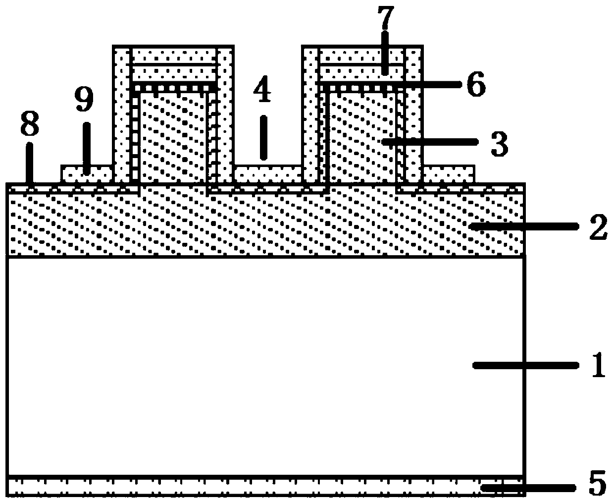
[0040] (3) On the diamond epitaxial layer 2, using metal as a mask, adopt dry etching method to etch strip-shaped channels to form a microstructure of periodic channels 4 and convex beams 3, such as Figure 4-3 shown;
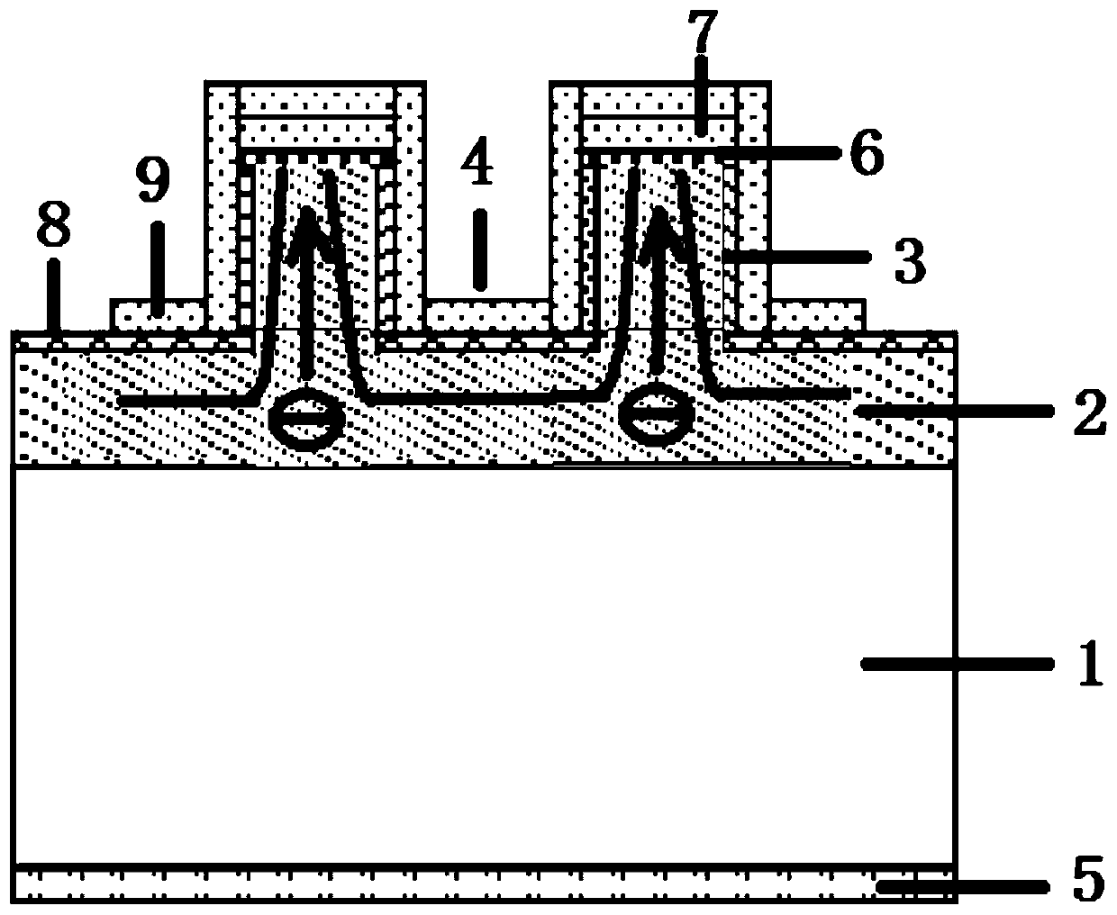
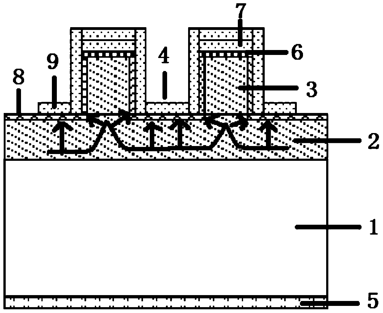
[0041] (4) make ohmic contact electrode 5 at the back side of p-type diamond substrate 1, as Figure 4-4 shown;
[0042] (5) The microstructure obtained in step (3) with periodic channels 4 interspersed wit...
Embodiment 1
[0048] (1) Clean the diamond substrate 1 using a standard acid-base cleaning process to remove the non-diamond phase on the surface, then use acetone, alcohol, and deionized water to clean the diamond substrate 1, and dry the diamond lining with nitrogen Bottom 1.
[0049] (2) An epitaxial layer 2 with a thickness of 0.5-60 microns is grown on the diamond substrate 1 by microwave plasma chemical vapor deposition technology.
[0050] (3) Use photolithography technology and magnetron sputtering technology to expose the channel to be etched, and use metal as a mask to cover the place that does not need to be etched.
[0051] (4) Etching the diamond epitaxial layer obtained in step (3) by dry etching to obtain a microstructure in which convex beams 3 and channels 4 are alternated, wherein the channel depth is 0.2-10 microns.
[0052] (5) The ohmic contact electrode 5 is fabricated on the back surface of the diamond epitaxial layer obtained in step (4).
[0053] (6) Utilize photo...
Embodiment 2
[0059] (1) Clean the diamond substrate 1 using a standard acid-base cleaning process to remove the non-diamond phase on the surface, then use acetone, alcohol, and deionized water to clean the diamond substrate 1, and dry the diamond lining with nitrogen Bottom 1.
[0060] (2) An epitaxial layer 2 with a thickness of 0.5-60 microns is grown on the diamond substrate 1 by microwave plasma chemical vapor deposition technology.
[0061] (3) The ohmic contact electrode 5 is fabricated on the back surface of the diamond epitaxial layer obtained in step (2).
[0062] (4) Use photolithography technology and magnetron sputtering technology to expose the trenches that need to be etched, and use metal as a mask in places that do not need to be etched.
[0063] (5) Etching the diamond epitaxial layer in step (4) by dry etching technology to etch out the microstructure of convex beams 3 and channels 4 alternately, wherein the depth of the channels is 0.2-10 microns.
[0064] (6) Reactive...
PUM
| Property | Measurement | Unit |
|---|---|---|
| thickness | aaaaa | aaaaa |
| breakdown field strength | aaaaa | aaaaa |
| breakdown voltage | aaaaa | aaaaa |
Abstract
Description
Claims
Application Information
 - Generate Ideas
- Intellectual Property
- Life Sciences
- Materials
- Tech Scout
- Unparalleled Data Quality
- Higher Quality Content
- 60% Fewer Hallucinations
Browse by: Latest US Patents, China's latest patents, Technical Efficacy Thesaurus, Application Domain, Technology Topic, Popular Technical Reports.
© 2025 PatSnap. All rights reserved.Legal|Privacy policy|Modern Slavery Act Transparency Statement|Sitemap|About US| Contact US: help@patsnap.com