SiC MPS diode containing NiO/SiC heterojunction
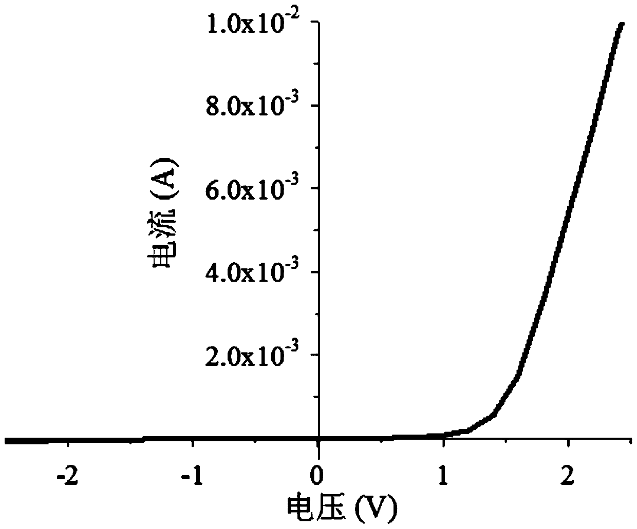
A diode and heterojunction technology, applied in the field of semiconductor devices, can solve problems such as large turn-on voltage, achieve low forward turn-on voltage, improve the effect of high on-state voltage drop, and high hole injection capability
- Summary
- Abstract
- Description
- Claims
- Application Information
AI Technical Summary
Problems solved by technology
Method used
Image
Examples
Embodiment 1
[0034] Hereinafter, the present invention will be further described in detail by taking a 650V 4H-SiC MPS diode containing NiO / SiC heterojunction as an example.
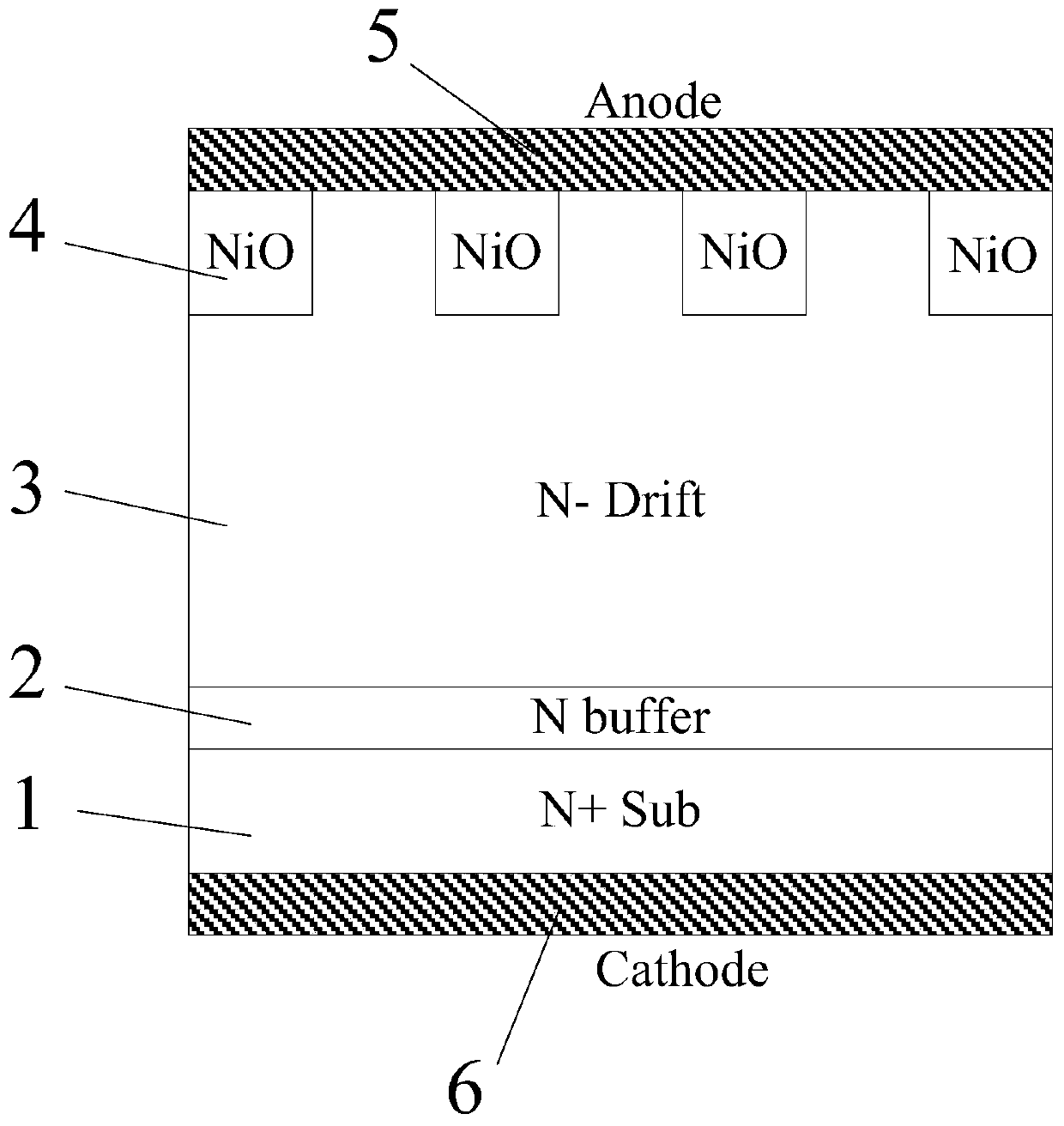
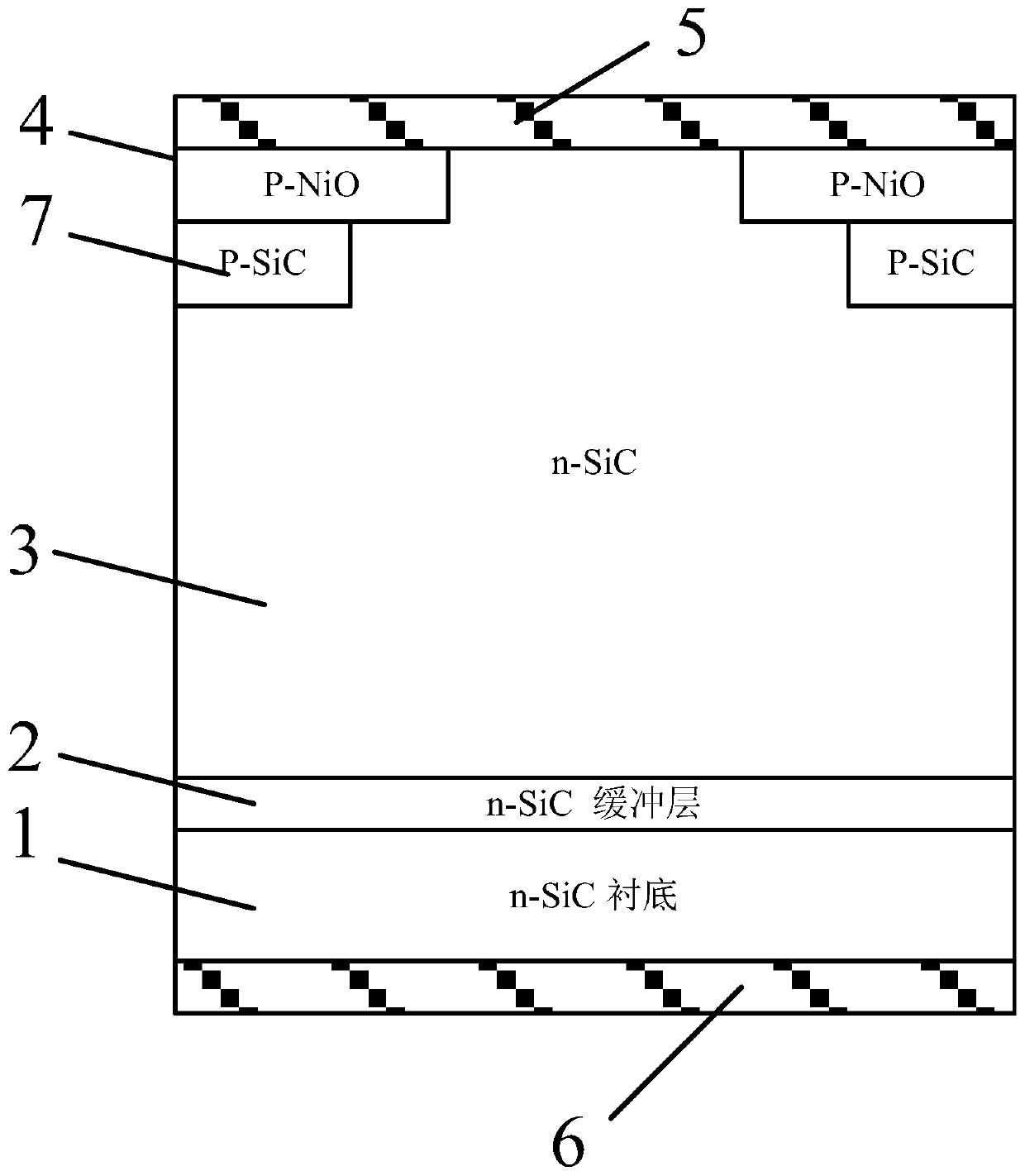
[0035] A kind of SiC MPS diode containing NiO / SiC heterojunction of the present invention, structure such as figure 1 As shown, a substrate 1 is included, and an n-SiC buffer layer 2 and an n-SiC drift region 3 are sequentially formed on the substrate 1. The upper end surface of the n-SiC drift region 3 is covered with an anode 5, and the lower end surface of the substrate 1 is covered with a cathode 6. A plurality of p-NiO junction regions 4 are inlaid at intervals on the upper surface of the n-SiC drift region 3 close to the anode 5 .
[0036] Wherein, the material of the p-NiO junction region 4 is p-type NiO, the thickness of the p-NiO junction region 4 is 0.5 μm, and the width of the p-NiO junction region 4 is 0.5 μm.
[0037]The material of the substrate 1 is n-type SiC, the thickness of the substrate 1 is 300 ...
Embodiment 2
[0043] Hereinafter, the present invention will be further described in detail by taking a 1200V 4H-SiC MPS diode containing NiO / SiC heterojunction as an example.
[0044] A kind of SiC MPS diode containing NiO / SiC heterojunction of the present invention, structure such as figure 1 As shown, a substrate 1 is included, and an n-SiC buffer layer 2 and an n-SiC drift region 3 are sequentially formed on the substrate 1. The upper end surface of the n-SiC drift region 3 is covered with an anode 5, and the lower end surface of the substrate 1 is covered with a cathode 6. A plurality of p-NiO junction regions 4 are inlaid at intervals on the upper surface of the n-SiC drift region 3 close to the anode 5 .
[0045] Wherein, the material of the p-NiO junction region 4 is p-type NiO, the thickness of the p-NiO junction region 4 is 0.5 μm, and the width of the p-NiO junction region 4 is 1.0 μm.
[0046] The material of the substrate 1 is n-type SiC, the thickness of the substrate 1 is 30...
Embodiment 3
[0052] Hereinafter, the present invention will be further described in detail by taking a 2700V 4H-SiC MPS diode containing NiO / SiC heterojunction as an example.
[0053] A kind of SiC MPS diode containing NiO / SiC heterojunction of the present invention, structure such as figure 1 As shown, a substrate 1 is included, and an n-SiC buffer layer 2 and an n-SiC drift region 3 are sequentially formed on the substrate 1. The upper end surface of the n-SiC drift region 3 is covered with an anode 5, and the lower end surface of the substrate 1 is covered with a cathode 6. A plurality of p-NiO junction regions 4 are inlaid at intervals on the upper surface of the n-SiC drift region 3 close to the anode 5 .
[0054] Wherein, the material of the p-NiO junction region 4 is p-type NiO, the thickness of the p-NiO junction region 4 is 0.5 μm, and the width of the p-NiO junction region 4 is 2.0 μm.
[0055] The material of the substrate 1 is n-type SiC, the thickness of the substrate 1 is 30...
PUM
| Property | Measurement | Unit |
|---|---|---|
| thickness | aaaaa | aaaaa |
| width | aaaaa | aaaaa |
| thickness | aaaaa | aaaaa |
Abstract
Description
Claims
Application Information
 - R&D Engineer
- R&D Manager
- IP Professional
- Industry Leading Data Capabilities
- Powerful AI technology
- Patent DNA Extraction
Browse by: Latest US Patents, China's latest patents, Technical Efficacy Thesaurus, Application Domain, Technology Topic, Popular Technical Reports.
© 2024 PatSnap. All rights reserved.Legal|Privacy policy|Modern Slavery Act Transparency Statement|Sitemap|About US| Contact US: help@patsnap.com


