Thin-film circuit electromagnetic shielding packaging method

A technology of electromagnetic shielding and thin-film circuits, applied in circuit devices, printed circuits, printed circuits, etc., can solve problems such as poor productivity, high circuit cost, and large volume, and achieve the effect of improving production efficiency and reducing costs

Active Publication Date: 2017-10-20
SOUTHWEST CHINA RES INST OF ELECTRONICS EQUIP
View PDF6 Cites 2 Cited by
  • Summary
  • Abstract
  • Description
  • Claims
  • Application Information

AI Technical Summary

Problems solved by technology

[0003] At present, the industry can see the method of using a metal shell surface-mounted on the front of the thin film circuit for packaging, but on the one hand, this method needs to integrate a large-area pad on the front, the circuit cost is high, and the volume is large. On the other hand, it needs to be welded and packaged piece by piece, and it can be produced in batches Poor sex

Method used


Image

  • Thin-film circuit electromagnetic shielding packaging method
  • Thin-film circuit electromagnetic shielding packaging method
  • Thin-film circuit electromagnetic shielding packaging method

Examples


specific Embodiment 1

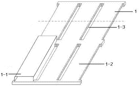
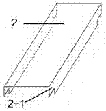
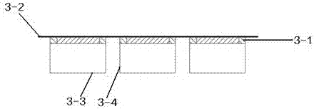
[0027] A thin film circuit electromagnetic shielding packaging method, such as figure 1 , figure 2 and image 3 As shown, the specific method is:

[0028] 1. Paste the front side of the substrate 1 that has completed the arrayed circuit arrangement on the high-temperature tape 3-2;

[0029] 2. Cover the back 3-3 and side 3-4 of the circuit chip with solder;

[0030] 3. Remove the high temperature tape;

[0031] 4. Select the metal cover 2 corresponding to the size of each circuit slice, fold down the metal cover and insert the edge sealing 2-1 into the substrate through cavity 1-3, so that the outer edge of the sealing edge is aligned with the bottom of the circuit chip, and the inner wall is aligned with the circuit close to;

[0032] 5. Turn over the clamped array structure so that the solder on the bottom surface is upward and fixed, and realize the batch welding and packaging of the metal cover and the thin film circuit chip through reflow soldering;

[0033] In the...

specific Embodiment 2

[0039] On the basis of the specific embodiment 1, the method further includes: obtaining the required independent devices by laser slicing after the welding is completed. After the overall welding is completed, the required self-shielding film circuit device can be obtained by dividing into pieces according to the circuit size.

specific Embodiment 3

[0040] On the basis of the specific embodiment 1 or 2, the specific method of coating the solder resist film on the front of each slice is: after the front of the substrate made of arrayed circuit arrangement is coated with a layer of solder resist film, the photolithography pattern Obtain the solder resist ring 3-1 of each circuit slice. After completion, use high temperature tape 3-2 to stick to the front of the substrate as a barrier layer.


PUM


Abstract

The invention provides a thin-film circuit electromagnetic shielding packaging method. The method concretely comprises the steps that step one, the front surface of a substrate completing array arrangement circuit manufacturing is adhered on a high temperature adhesive tape; step two, the solder is covered on the back surface and the side surface of a circuit wafer; step three, the high temperature adhesive tape is removed; step four, a metal seal cover having the corresponding size with that of each circuit sub-wafer is selected, and the metal seal cover is downwardly folded and sealed to be embedded in the through cavity of the substrate so that the sealed external edge is enabled to be aligned with the bottom part of the circuit wafer and the internal wall is enabled to be closely fit with the circuit; and step five, the clamped array structure is overturned so that the bottom solder is enabled to be upward and fixed, and batch soldering and packaging of the metal seal cover and the thin-film circuit wafer can be realized through reflow soldering. Compared with the methods in the prior art, device level radio frequency signal electromagnetic shielding can be realized, the volume weight is reduced for more than 90% and the cost is reduced for more than 20% in comparison with the mechanical processing metal shell packaging mode. Meanwhile, the batch device assembling mode is adopted and automatic assembling can be supported so that the production efficiency can be enhanced for about 20%.

Description

technical field [0001] The invention relates to an electromagnetic shielding packaging method for a thin film circuit, in particular to an electromagnetic shielding packaging method for a thin film circuit that is suitable for side welding of a metal upper cover and realizes the radio frequency signal shielding function; it is suitable for thin film circuit integration, welding, and electromagnetic shielding and other process technologies, especially device-level processes. Background technique [0002] In order to solve the problem of radio frequency signal interference, the traditional microwave thin film circuit adopts the method of placing the circuit chip in the metal cavity and shielding it through the metal shell. This can achieve a better shielding effect, but this method has the disadvantage of excessive circuit volume and weight, which greatly affects the miniaturization and integration of microwave thin film circuits. In the application of new electronic equipmen...

Claims


Application Information

Patent Timeline
Patent Type & Authority Applications(China)
IPC IPC(8): H05K1/02H05K3/34
CPCH05K1/0216H05K3/34H05K2201/10371H05K2203/1305
Inventor 王文博秦跃利王春富李彦睿周俊
Owner SOUTHWEST CHINA RES INST OF ELECTRONICS EQUIP
Why Eureka
Try Eureka