Packaging structure and method for electromagnetic shielding of chip
A technology of electromagnetic shielding and packaging method, which is applied to circuits, electrical components, electrical solid devices, etc., and can solve the problems of large volume, high difficulty and high preparation cost of the packaging body.
- Summary
- Abstract
- Description
- Claims
- Application Information
AI Technical Summary
Problems solved by technology
Method used
Image

Examples
Embodiment 1
[0033] Embodiments of the present invention provide a packaging structure for implementing electromagnetic shielding on chips, such as Figure 5G As shown, the package structure for realizing electromagnetic shielding of chips includes a chip to be shielded 50 , a molding layer 70 , at least one conductive bridge 60 , and a conductive layer 30 .
[0034] The molding layer 70 covers the sidewall of the chip to be shielded 50 and exposes the pad of the chip to be shielded 50 .
[0035] The conductive bridge 60 includes at least one conductive metal structure, the conductive bridge 60 penetrates the molding layer 70 , and the two ends of the conductive metal structure in the conductive bridge 70 are respectively exposed on both sides of the molding layer 70 . The conductive bridge 60 can be a separate conductive metal wire or a conductive metal sheet (this situation is not shown in the accompanying drawings of the present application; based on the limitation of the manufacturing ...
Embodiment 2
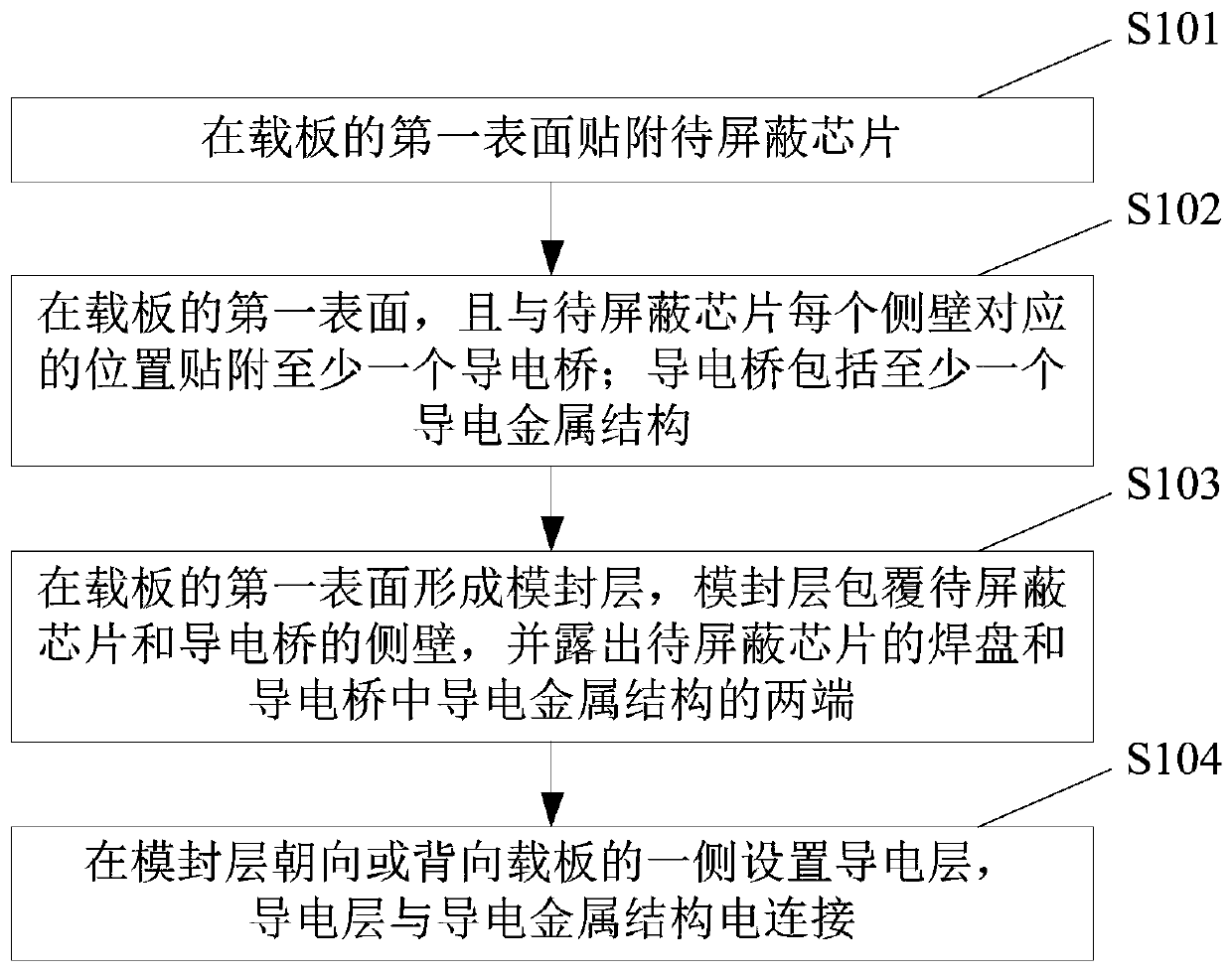
[0044] figure 1 A flow chart of a packaging method for implementing electromagnetic shielding for a chip according to an embodiment of the present invention is shown, and the packaging method can be used to manufacture the packaging structure described in Embodiment 1 or any optional implementation manner thereof. Such as figure 1 As shown, the method includes the following steps:
[0045] S101: attaching the chip to be shielded on the first surface of the carrier board.
[0046] S102: Attach at least one conductive bridge on the first surface of the carrier board at a position corresponding to each sidewall of the chip to be shielded; the conductive bridge includes at least one conductive metal structure.
[0047] Such as Figure 5D As shown, 10 is a carrier board, and 50 is a chip to be shielded. In this step S101, the method of attaching the chip 50 to be shielded can be as follows Figure 5A and Figure 5D Shown: (In one embodiment, Figure 5A and Figure 5D The co...
Embodiment 3
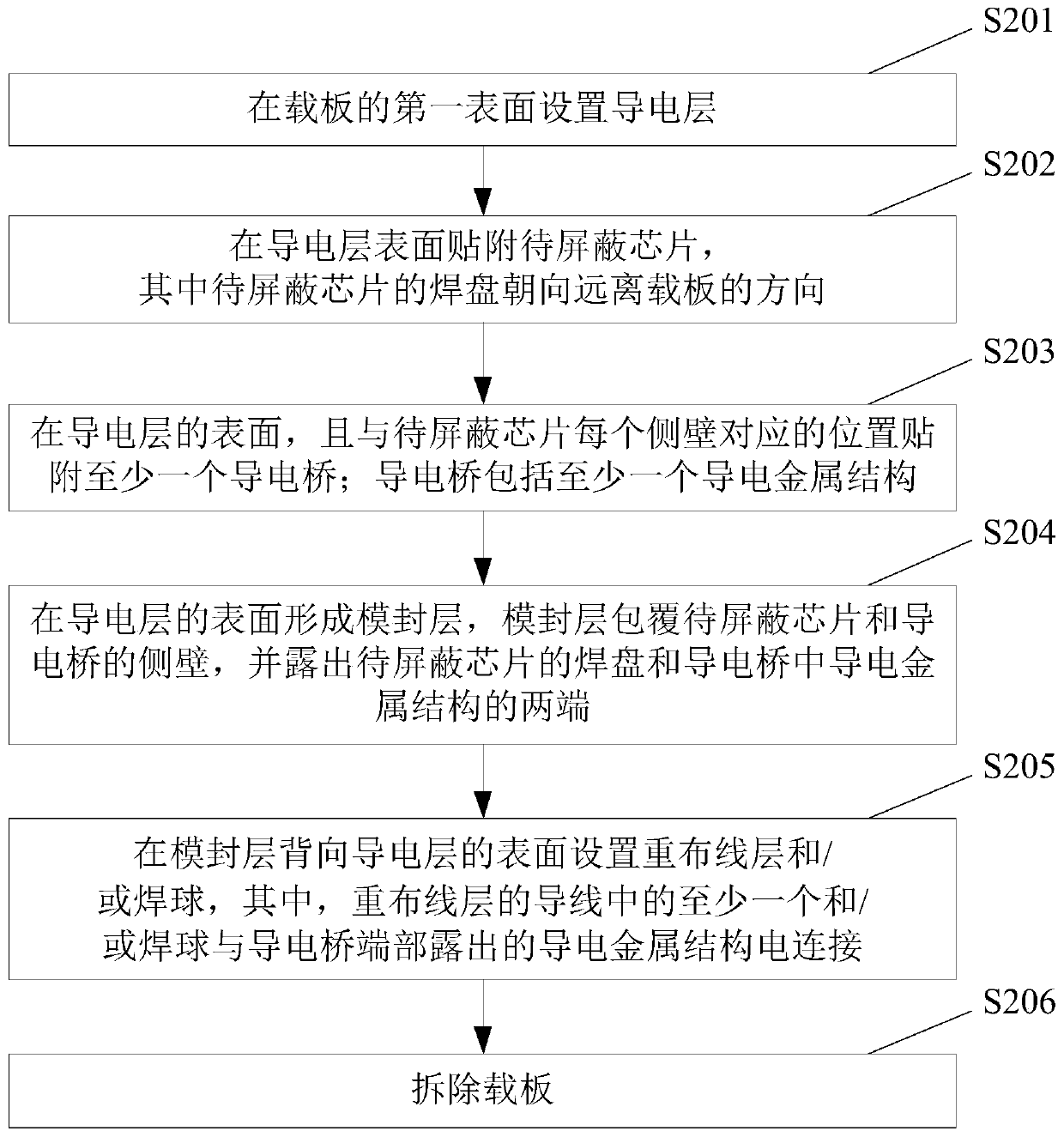
[0060] figure 2 A flow chart of another packaging method for implementing electromagnetic shielding for chips according to an embodiment of the present invention is shown, and the packaging method can be used to manufacture the packaging structure described in Embodiment 1 or any optional implementation manner thereof. Such as figure 2 As shown, the method includes the following steps:
[0061] S201: Disposing a conductive layer on the first surface of the carrier.
[0062] Such as Figure 5A As shown, 10 is a carrier board, and 30 is a conductive layer. For details, refer to step S104 in the third embodiment.
[0063] S202: attaching the chip to be shielded on the surface of the conductive layer, wherein the pads of the chip to be shielded face away from the carrier board.
[0064] S203: Attach at least one conductive bridge on the surface of the conductive layer at a position corresponding to each sidewall of the chip to be shielded; the conductive bridge includes at ...
PUM
 Abstract
Description
Claims
Application Information
 - R&D
- Intellectual Property
- Life Sciences
- Materials
- Tech Scout
- Unparalleled Data Quality
- Higher Quality Content
- 60% Fewer Hallucinations
Browse by: Latest US Patents, China's latest patents, Technical Efficacy Thesaurus, Application Domain, Technology Topic, Popular Technical Reports.
© 2025 PatSnap. All rights reserved.Legal|Privacy policy|Modern Slavery Act Transparency Statement|Sitemap|About US| Contact US: help@patsnap.com