PCB manufacturing method and PCB

A manufacturing method and signal hole technology, applied in printed circuit manufacturing, reduction of crosstalk/noise/electromagnetic interference (, printed circuit, etc.), can solve problems such as high wiring density and failure to meet customer design requirements

Active Publication Date: 2019-10-01
DONGGUAN SHENGYI ELECTRONICS
View PDF3 Cites 2 Cited by
  • Summary
  • Abstract
  • Description
  • Claims
  • Application Information

AI Technical Summary

Problems solved by technology

However, as the signal wavelength is getting shorter and shorter, the area of ​​the PCB is getting smaller and the wiring density is getting higher and higher, and the spacing of the shielding holes is reduced synchronously to ensure the quality of the shielding. Meet customer design requirements

Method used


Image

  • PCB manufacturing method and PCB
  • PCB manufacturing method and PCB
  • PCB manufacturing method and PCB

Examples


Embodiment 1

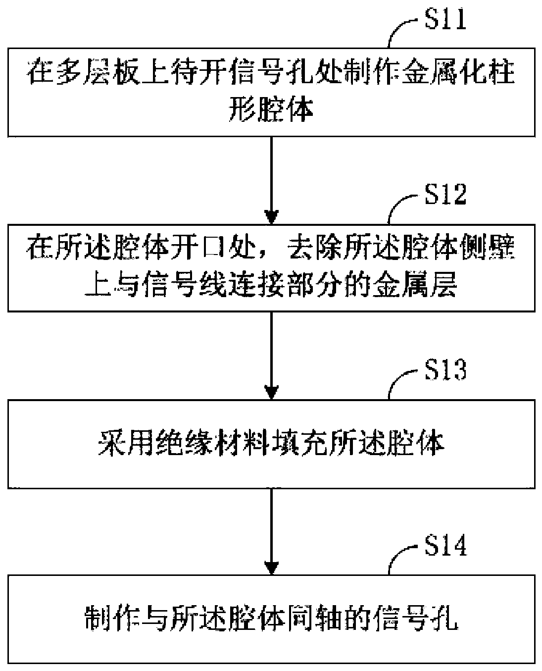
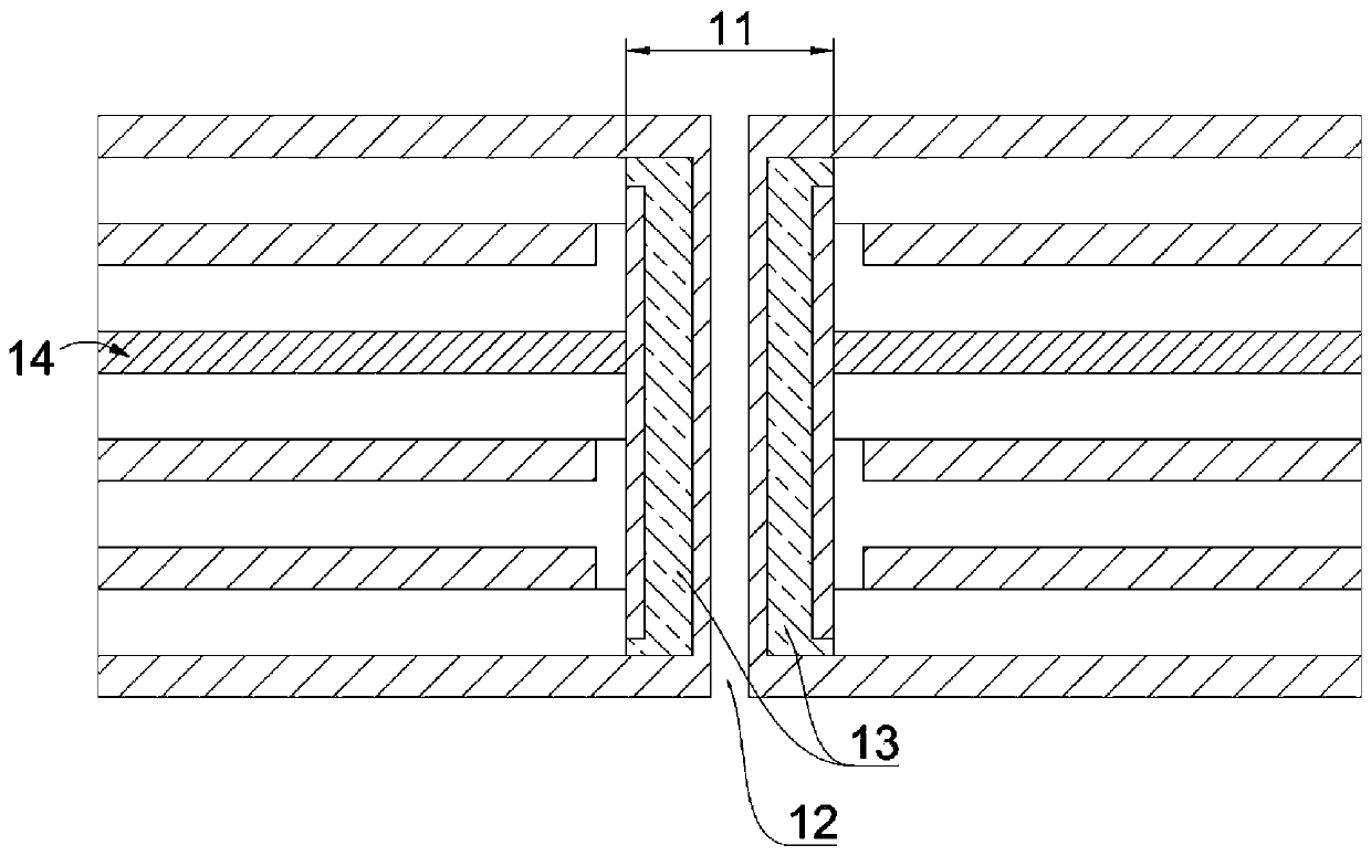
[0042] This embodiment provides a method for manufacturing a PCB. The electromagnetic shielding of the signal holes is realized by arranging the signal holes in the metallized cylindrical cavity, which is suitable for high-density PCBs that cannot be provided with shielding holes.

[0043] figure 1 It is a flow chart of the PCB manufacturing method provided by Embodiment 1 of the present invention. Such as figure 1 As shown, the manufacturing method of PCB includes the following steps:

[0044] S11, making a metallized cylindrical cavity at the signal hole to be opened on the multi-layer board.

[0045] Before step S11, remove the copper layer at the position where the cavity is to be made except for the inner layer of the copper layer on each layer of the core board, and the size of the removed copper layer is larger than the cross-sectional size of the cavity; The core boards of each layer are laminated with the prepreg and pressed into a multi-layer board.

[0046] Maki...


PUM


Abstract

The invention discloses a PCB manufacturing method and a PCB, which relate to the field of printed circuit board manufacturing. The PCB manufacturing method includes the following steps: making a metalized cylindrical cavity at a signal hole to be opened in a multilayer board; removing a metal layer of a part connected with a signal line on the side wall of the cavity at the opening of the cavity;filling the cavity with an insulating material; and making a signal hole coaxial with the cavity. By arranging the signal hole in the metalized cylindrical cavity to realize electromagnetic shieldingof the signal hole, the problem that the electromagnetic leakage of the signal hole cannot be eliminated and the signal quality is thus reduced because there is no space to arrange a shielding hole in a high-density PCB is solved.

Description

technical field [0001] The invention relates to the field of printed circuit board manufacturing, in particular to a method for manufacturing a PCB and the PCB. Background technique [0002] In high-frequency PCB design, it is inevitable to use metallized holes for interlayer exchange of electromagnetic signals. According to the electromagnetic principle, in order to eliminate the electromagnetic leakage of the signal holes on the PCB in the core board layer and shield the influence of other electromagnetic waves on the signal quality, it is necessary to use dense holes with hole spacing smaller than the signal wavelength to form a shielding wall to ensure the signal transmission quality. However, as the signal wavelength is getting shorter and shorter, the area of ​​the PCB is getting smaller and the wiring density is getting higher and higher, and the spacing of the shielding holes is reduced synchronously to ensure the quality of the shielding. Meet customer's design req...

Claims


Application Information

Patent Timeline
Patent Type & Authority Applications(China)
IPC IPC(8): H05K1/02H05K1/11H05K3/00
CPCH05K1/0219H05K1/116H05K3/0094H05K2201/0959
Inventor 赵康纪成光袁继旺陈正清
Owner DONGGUAN SHENGYI ELECTRONICS
Why Eureka
Try Eureka